


 A universal AC/DC booster, audio amplifier and line driver can be used in sensor circuits, audio signal generators, electrical guitars and so on. Most of these applications need high input impedance (for example, 10-mega-ohm), low quiescent current, output current limiting function, low total harmonic distortion (THD) and intermodulation distortion (IMD), and are capable of driving loads as low as 32-ohm, like headphones and high-impedance loudspeakers.
This circuit produces ±300mA output current and 20Vpp (±10V) output voltage with power supply of ±15V. It is simple and useful for a large variety of applications.
Circuit and working
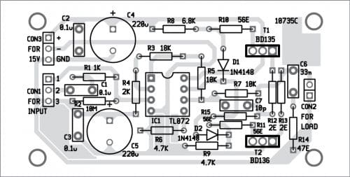
The circuit diagram of the universal circuit is shown in Fig. 1. It is built around op-amp TL072 (IC1), transistor BD135 (T1), transistor BD136 (T2), diodes 1N4148 (D1 and D2) and a few other components.


The circuit has two operational amplifier stages (A1 and A2). Both stages are built around dual JFET operational amplifier TL072 (IC1). You may replace IC1 with TL082, LF412, LF353, etc.
You can apply AC or DC, or audio input signal to connector CON1. Capacitor C1 is used if the circuit is used as AC booster or audio amplifier. Input resistance is determined by resistor R2 (10-mega-ohm), which can be set to any appropriate value.

Op-amp A1 of IC1 operates as DC amplifier whose gain is determined by the following relationship:
Av1=1+R3/R4=10
You may use any appropriate gain that is more than or equal to 1
Op-amp A2 of IC1 operates as DC amplifier whose gain is determined by the following relationship:
Av2=–R7/R5=–1
Total gain Av of the circuit is Av1 x Av2=10 x (-1)=–10
Output stage is built around two bipolar transistors (T1 and T2). R8, D1, D2, R9 and R15 are used to reduce THD and IMD of the amplifier. Resistor R15 should have the minimum applicable value to have minimal THD and IMD.
Resistors R12 and R13 operate as current-limiting elements. Maximum output current is determined by the following relationship:
Imax=0.68V/R12=0.68V/R13 =340mA
R10, R11, C6 and R14 reduce THD and increase stability of the circuit.
Construction and testing
An actual-size PCB layout of the circuit is shown in Fig. 3 and its components layout in Fig. 4. After assembling the circuit on the PCB, connect a ±15V power supply across CON3.
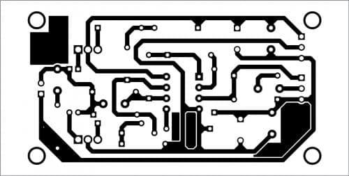
Download PCB and Component layout PDFs: click here
You can give three types of inputs—DC, AC and audio—across CON1. Connect DC input across terminals 1 and 3 of CON1, or AC input across terminals 2 and 3 of CON1. Connect audio signal input from the mobile/laptop/PC across terminals 2 and 3 of CON1.
The circuit can be tested with a resistive load of 100-ohm connected across CON2 using a power supply of ±15V and AC input signal of ±1Vpp, which should give a total gain of -10. The circuit does not require any adjustment. You may need small heat-sinks for T1 and T2 with thermal resistance around 35°C/W.
Petre Tzv Petrov was a researcher and assistant professor in Technical University of Sofia, Bulgaria and expert-lecturer in OFPPT (Casablanca), Kingdom of Morocco. Now he is working as an electronics engineer in the private sector in Bulgaria.