


Understanding optronic sensors and related sensor systems is essential to understanding the design and operation of a large number of defence systems. Hence this six-part article series starts with an overview of these sensors.
Optronic sensors constitute the heart of a variety of systems ranging from simple gadgets like light meters to the most complex of military systems like precision-guided munitions, laser rangefinders, target trackers, remote sensing systems, navigation sensors, sniper and explosive detectors, fibre-optic and laser-based communication systems, night vision devices, Lidar and spectroscopic sensors. While individual photosensors such as PIN photodiodes and avalanche photodiodes find applications in military optronic systems including laser rangefinders and target designators, Lidar sensors and navigation sensors, sensor arrays such as complementary metal-oxide semiconductor (CMOS), charge-coupled device and avalanche photodiodes are at the core of imaging sensor systems including Ladar sensors, night vision devices, laser and imaging infrared seekers.

Types of photosensors
Photosensors are classified into two major categories: Photoelectric and thermal. Photoelectric sensors are further of two types: Devices that depend on the external photo effect for their operation and devices that make use of some kind of internal photo effect.
Photo-emissive sensors are based on external photo effect. Common photo-emissive sensors include non-imaging sensors such as vacuum photo cells and photomultiplier tubes, and imaging sensors such as image intensifier tubes.
Photoconductors and junction-type photosensors use internal photo effect. Photoconductors are bulk semiconductor devices whose resistance decreases with increase in incident light intensity. These are also known by the name of photoresistors, light-dependent resistors and photocells.
Junction-type photosensors are further amplifying and non-amplifying type. Amplifying-type junction photosensors include phototransistors, photothyristors and photo-field-effect transistors (FETs). Non-amplifying types of junction photosensors include photodiodes, solar cells, CMOS and charge-coupled devices. CMOS and charge-coupled device are imaging sensors. The category of thermal sensors includes thermocouple (or thermopile) type sensors, bolometric sensors and pyroelectric sensors.
Thermal sensors absorb incident radiation and operate on the resulting temperature rise, whereas photoelectric sensors are based on quantum effect. Compared to photoelectric sensors, thermal sensors are sluggish in their response to the incident radiation. However, these offer a much wider operational wavelength band than photoelectric sensors.
Characteristic parameters
Major parameters used to characterise the performance of photosensors include responsivity, noise equivalent power (NEP), sensitivity (usually measured as detectivity or D*), quantum efficiency, response time and noise.
Responsivity is the ratio of electrical output to radiant light input determined in the linear region of response. It is measured in amperes per watt (A/W) or V/W if the photosensor produces a voltage output rather than a current output. Responsivity is a function of the incident radiation’s wavelength and band-gap energy. Spectral response is a related parameter. It is a curve that shows variation of responsivity as a function of wavelength.
Most photoelectric sensors have a narrow spectral response, whereas most thermal sensors have a wide spectral response. As an example, spectral responses of silicon, germanium, indium-gallium-arsenide photodiodes are in the range of 200-1100nm, 500-1900nm and 700-1700nm, respectively, in comparison to thermistors’ 0.5-10µm.
Silicon photodiodes exhibit a response from ultraviolet through visible and into near infrared part of the spectrum. With silicon having band-gap energy of 1.12eV at room temperature, its spectral response peaks in the near infrared region between 800nm and 950nm. Peak responsivity figures for silicon PIN photodiodes are in the range of 0.4-0.6A/W in comparison to avalanche photodiodes’ 40-80A/W. Thermal sensors have poorer responsivity than photoelectric sensors. For instance, the responsivity of pyroelectric sensors is in the range of 0.5-5µA/W.
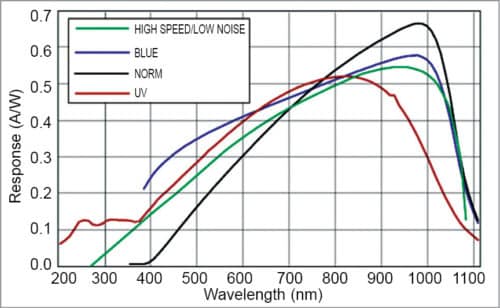
The shape of the spectral response curve of silicon photosensors, particularly in blue and UV parts of the spectrum, can be altered by choosing an appropriate manufacturing process. Fig. 1 shows typical spectral response curves of normal, blue-enhanced and UV-enhanced, and low-noise silicon photodiodes. Low-noise spectral response corresponds to photodiodes’ photovoltaic mode of operation wherein no external bias is applied to the photodiode. Since dark current is a function of bias voltage magnitude, photovoltaic mode of operation eliminates dark current as a source of noise. In this case, NEP will be lower, thereby allowing greater sensitivity at lower wavelengths but at the cost of slightly lower responsivity at higher wavelengths.
Silicon becomes transparent to radiations of longer than 1100nm wavelength. On the contrary, wavelengths in ultraviolet region are absorbed in the first 100nm thickness of silicon. Even the most careful surface preparation leaves some surface damage, which reduces collection efficiency for this wavelength. High absorption coefficient of silicon in blue- and UV-enhanced spectral region leads to carrier generation within heavily doped p+ (or n+) contact surface of P-N and PIN photodiodes. This causes rapid decrease in quantum efficiency of this region due to shorter lifetime and surface recombination.
Spectral response of photodiodes in blue- and UV-enhanced region is enhanced by minimising near-surface recombination. This is achieved by using techniques such as thin and highly graded p+ (or n+ or metal Schottky) contacts, lateral collection to minimise percentage of heavily-doped surface area and passivation layer. A passivation layer such as silicon nitride, silicon dioxide or titanium dioxide can reduce surface recombination.
Anti-reflection coatings may be used to enhance responsivity to about 25 per cent at the required wavelength, but this leads to reduced efficiency at other wavelengths that these reflect. Package window also plays an important role in shaping the spectral response. The standard glass window absorbs wavelengths shorter than 300nm. For UV detection, a fused silica or UV transmitting glass window is used. Various filter windows are also available to tailor the spectral response for an application. Optical filters can also be added to change the spectral response. A common example is the use of a specific filter to modify the normal silicon response to approximate the spectral response of the human eye.
Due to improved charge-collection efficiency in photodiodes, responsivity increases slightly with applied reverse bias. It also exhibits dependence on temperature variations due to variation in band-gap energy. The band-gap energy varies inversely with the change in temperature.
The term ‘responsivity’ should not be confused with ‘sensitivity’. Sensitivity is the lowest detectable light level that is typically determined by detection noise. It is also significantly influenced by the required detection bandwidth. Also, a photosensor should ideally be operated in a spectral region where its responsivity is not far below the highest possible value, because this leads to the lowest possible detection noise and thus to a high signal-to-noise ratio and high sensitivity.
Noise equivalent power (NEP) is the input power to a sensor that generates an output signal current equal to the total internal noise current of the device, which implies signal-to-noise ratio of 1 (one). In other words, it is the minimum detectable radiation level of the sensor. Noise power and thus noise-equivalent power depend on the assumed detection bandwidth.
If one were to use the full detection bandwidth of a device to compute NEP, the NEP would not allow a fair comparison of sensors with different bandwidths. Therefore it is a common practice to assume a bandwidth of 1Hz, which is usually far below the detection bandwidth. NEP is usually specified in units of W/Hz rather than watts.
Detectivity of a sensor is the reciprocal of its NEP. Sensors with higher value of detectivity are more sensitive. Detectivity, like NEP, depends upon noise bandwidth and sensor area. To eliminate these factors, a normalised figure of detectivity, referred to as D* (Dee-star), is used. It is defined as the detectivity normalised to an area of 1cm2 and noise bandwidth of 1Hz.
Quantum efficiency is the ratio of the number of photoelectrons released to the number of incident light photons absorbed. It is the percentage of input radiation power converted into photo current. It is expressed as rise/fall time parameter in photoelectric sensors and as time constant parameter in thermal sensors. Rise and fall times are the time durations for the output to change from 10 per cent to 90 per cent, and 90 per cent to 10 per cent of the final response, respectively. Rise/fall time parameter determines the highest signal frequency to which a sensor can respond. Time constant is defined as the time required by the output to reach 63 per cent of the final response from zero initial value.
Noise is the most critical factor in designing sensitive radiation detection systems. Noise in these systems is generated in photosensors, radiation sources and post-detection circuitry. Photosensor noise mainly comprises Johnson noise, shot noise, generation-recombination noise and flicker noise.
Johnson noise, also known as Nyquist noise or thermal noise, is caused by thermal motion of charged particles in a resistive element. The RMS value of noise voltage depends on the resistance value, temperature and system bandwidth.
Shot noise in a photosensor is caused by the discrete nature of photoelectrons generated. It is related to the statistical fluctuation of both the dark current and the photo current. It depends on the average current through the photosensor and system bandwidth. It is the dominant source of noise in the case of photodiodes operating in photoconductive mode.
Generation-recombination noise is caused by fluctuation in current generation and recombination rates in a photosensor. This type of noise is predominant in photoconductive sensors operating at infrared wavelengths.
Flicker noise, or 1/f noise, occurs in all conductors where the conducting medium is not a metal and all semiconductor devices that require bias current for their operation. Its amplitude is inversely proportional to the frequency. Flicker noise is usually predominant at frequencies below 100Hz.
Photoconductors
Photoconductors—also referred to as photoresistors, light-dependent resistors (LDRs) and photocells—are semiconductor photosensors whose resistance decreases with increase in incident light intensity. These are bulk semiconductor devices with no p-n junction. The resistance change in a photoconductor is of the order of 6 decades, ranging from few tens of mega-ohms under dark conditions to few tens or hundreds of ohms under bright light conditions. Other features include wide dynamic response, spectral coverage from ultraviolet to far infrared, and low cost. However, photoconductors have response time of the order of hundreds of milliseconds.
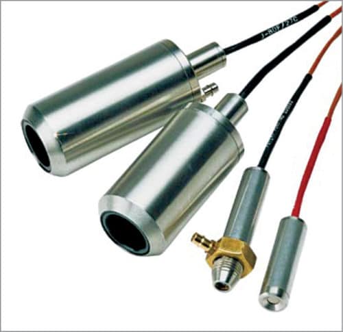
Commonly used materials for photoconductors are cadmium-sulphide (CdS), lead-sulphide (PbS), lead-selenide (PbSe), mercury-cadmium-telluride (HgCdTe) and germanium-copper (Ge:Cu). Inexpensive CdS photoconductors are used in many consumer items like camera light meters, clock radios, security alarms, street lights and so on. On the other hand, Ge:Cu cells are used for infrared astronomy and infrared spectroscopy. Fig. 2 shows some representative photoconductors.

Photoconductors are further classified as intrinsic or extrinsic depending upon whether an external dopant has been added or not to the semiconductor material. Intrinsic photoconductors operate at shorter wavelengths as electrons have to jump from valence to conduction band. Extrinsic photoconductors have a spectral response covering longer wavelengths.
A simple application circuit using a photoconductor would be a potential divider arrangement comprising a fixed resistor and photoconductor. A fixed DC voltage is applied to the potential divider and the voltage appearing across either the fixed resistor or the photoconductor is taken as a measure of light intensity. A better option would be to use the photoconductor in conjunction with an operational amplifier wired either as a trans-impedance amplifier or voltage-mode amplifier. This gives better responsivity and higher output voltage.
Photodiodes
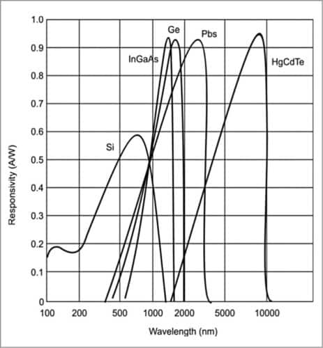
Photodiodes are junction-type semiconductor light sensors that generate current or voltage when p-n junction in the semiconductor is illuminated by light of sufficient energy. Spectral response of the photodiode is a function of the band-gap energy of the material used in its construction. Photodiodes are mostly constructed using silicon, germanium, indium-gallium-arsenide (InGaAs), lead-sulphide (PbS) and mercury-cadmium-telluride (HgCdTe). Fig. 3 shows spectral characteristics of these photodiodes.
Types of photodiodes
Depending upon construction, there are several types of photodiodes. These include p-n photodiodes, PIN photodiodes, Schottky-type photodiodes and avalanche photodiodes.
p-n photodiodes comprise a p-n junction. When light with sufficient energy strikes the photodiode, its electrons are pulled up into conduction band, leaving behind holes in valence band. These electron-hole pairs occur throughout p-layer, depletion layer and n-layer materials. When the photodiode is reverse biased, photo-induced electrons move down the potential hill from p-side to n-side. Similarly, photo-induced holes add to the current flow by moving across the junction to p-side. Shorter wavelengths are absorbed at the surface, while longer wavelengths penetrate deep into the diode. p-n photodiodes are used for precision photometry applications like medical instrumentation, analytical instruments, semiconductor tools and industrial measurement systems.
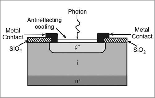
In PIN photodiodes, an extra high-resistance intrinsic layer is added between p and n layers (Fig. 4). This reduces the transit or diffusion time of photo-induced electron-hole pairs, which, in turn, improves the response time. PIN photodiodes feature low capacitance and therefore high bandwidth, which makes them suitable for high-speed photometry as well as optical communication applications.
Single-element PIN photodiodes, quadrant photodiodes, and one- and two-dimensional arrays of photodiodes find extensive application in a variety of sensor systems for military applications. Prominent among these include laser warning sensor suites on armoured fighting vehicles and airborne platforms, laser seekers in laser-guided munitions, laser receivers in laser communication systems and focal-plane arrays in Ladar sensors.
Photodiodes and photodiode arrays integrated with peripheral components such as low-noise pre-amplifier circuits are also available in a single package.
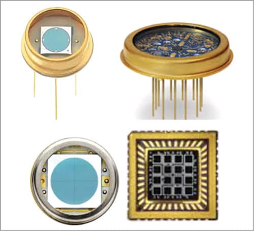
Fig. 5 shows single, quad and two-dimensional arrays of PIN photodiodes in some of the more common package configurations. Photodiodes are available in many more packages including customised ones. In Schottky type photodiodes, a thin gold coating is sputtered onto the n-material to form a Schottky-effect p-n junction. Schottky photodiodes have enhanced UV response.
Avalanche photodiodes are high-speed, high-sensitivity photodiodes utilising an internal gain mechanism that functions by applying a relatively higher reverse bias voltage than PIN photodiodes. These have fast response times similar to that of PIN photodiodes. Also, responsivity of avalanche photodiodes (40-80A/W) is around 100 times more than silicon PIN photodiodes (0.4-0.6A/W). Moreover, avalanche photodiodes offer an excellent signal-to-noise ratio that is comparable to the value offered by photomultiplier tubes. Hence these are used in a variety of applications requiring high sensitivity, such as long-distance optical communication and optical distance measurement. Military laser rangefinders based on time-of-flight principle have their receivers’ front end invariably employing a silicon or indium-gallium-arsenide avalanche photodiode depending upon whether it is an Nd:YAG laser rangefinder or an eye-safe laser rangefinder. Just like PIN photodiodes, avalanche photodiodes are available as single detectors as well as linear or two-dimensional arrays in similar package configurations.
Photodiodes can be operated in two modes: photovoltaic and photoconductive. In photovoltaic mode, no bias voltage is applied and due to the incident light, a forward voltage is produced across the photodiode. In photoconductive mode, a reverse bias voltage is applied across the photodiode. This widens the depletion region, resulting in higher speed of response.
As a thumb rule, all applications requiring a bandwidth less than 10kHz can use photodiodes in photovoltaic mode. For all other applications, photodiodes are operated in photoconductive mode. Moreover, the linearity of a photodiode improves when it is operated in photoconductive mode. However, noise current of the photodiode increases when it is operated in photoconductive mode. This is due to the reverse saturation current, referred to as dark current, flowing through the photodiode. The value of dark current is typically in the range of 1-10nA at a specified reverse bias voltage. When the photodiode is operated in photovoltaic mode, dark current is zero.
Application circuits
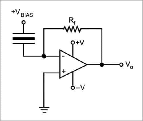
A commonly used application circuit employing PIN photodiode in photovoltaic mode is shown in Fig. 6. The output voltage is given by Idet×R, where Idet is the current through the photodiode.
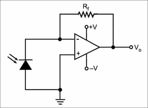
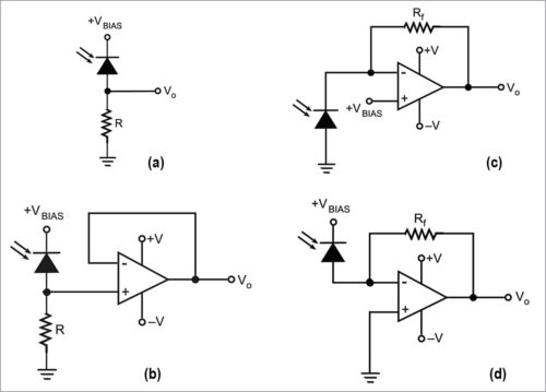
Fig. 7 shows four possible circuits of PIN photodiodes in photoconductive mode. Fig. 7(a) shows the basic circuit with no amplification. In Fig. 7(b) the operational amplifier is used as a voltage amplifier, whereas in Figs 7(c) and (d) the operational amplifier is used in transimpedance mode. For the circuit in Fig. 7(b), output voltage and effective resistance across the photodiode are (Idet×R) and R, respectively. Idet is the current flowing through the photodiode. Output voltage and effective resistance across the photodiode in Figs 7(c) and (d) are (Idet×Rf) and Rf/A, respectively, where Idet is photodiode current and A is open-loop gain of the operational amplifier. Circuits in Figs 7(c) and (d) offer better linearity.
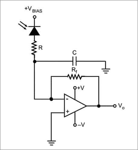
Avalanche photodiodes are also connected in a similar manner as discussed above, except that a much higher reverse bias voltage is required for their operation. Also, their power consumption during operation is much higher than PIN photodiodes and is given by the product of input signal, sensitivity and reverse bias voltage. Hence a protective resistor is added to the bias circuit (Fig. 8) or a current-limiting circuit is used.
Solar cells
Solar cells operate very similar to photodiodes in photovoltaic mode. These operate on the principle of photovoltaic effect. As mentioned above, due to photovoltaic effect, an open-circuit voltage develops across a p-n junction when it is exposed to light, which is solar radiation in the case of a solar cell. This open-circuit voltage leads to the flow of electric current through a load resistance connected across it (Fig. 9).
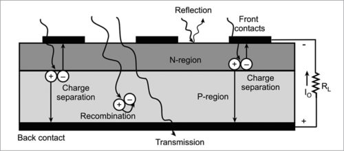
As shown in Fig. 9, the impinging photon energy causes generation of electron-hole pairs. These electron-hole pairs either recombine and vanish, or start drifting in opposite directions with electrons moving towards n-region and holes moving towards p-region. The accumulation of positive and negative charge carriers constitutes the open-circuit voltage. This voltage can cause a current through the external load or, when the junction is shorted, a short-circuit current whose magnitude is proportional to the input light intensity.
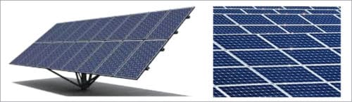
The voltage output and the current delivery capability of an individual solar cell are very small for use as an electrical power input to any system. As an example, a typical solar cell would produce 500mV output with load current capability of about 150mA. A series-parallel arrangement of solar cells gives the desired output voltage with required power delivery capability. Series combination enhances the output voltage, while parallel combination enhances the current rating. Fig. 10 shows some representative solar cell panels.
Solar cell efficiency is the ratio of maximum electrical solar cell power to the radiant light power on the solar cell area. The efficiency figure for some crystalline solar cells is in excess of 20 per cent. Silicon is most commonly used semiconductor material for solar cells. Both crystalline and amorphous forms of silicon are used for the purpose. Another promising material for solar cells is gallium-arsenide (GaAs). Gallium-arsenide solar cells, when perfected, will be light-weight and more efficient.
Photoemissive sensors
Photoemissive sensors rely on external photo effect, wherein photo-generated electrons travel beyond physical boundaries of the material. Some of the commonly used photoemissive photosensors include vacuum photodiodes, photomultiplier tubes and image-intensifier tubes.
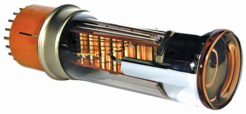
Photomultiplier tubes are extremely sensitive photosensors operating in the ultraviolet, visible and near-infrared spectrum. These have internal gain of the order of 108 and can detect even a single photon of light. They are constructed from a glass vacuum tube that houses a photocathode, several dynodes and an anode. When incident photons strike the photocathode, electrons are produced as a result of the photoelectric effect. These electrons accelerate towards the anode and in the process, electron multiplication takes place due to secondary emission from dynodes.
Salient features of photomultiplier tubes include low noise, high-frequency response and large active area. By virtue of these features, photomultiplier tubes are used in nuclear and particle physics, astronomy, medical imaging and motion-picture film scanning. Fig. 11 shows a representative photomultiplier tube.
Thermal sensors
Thermal sensors absorb radiation, which causes a change in temperature and hence physical or electrical property of the sensor. In other words, thermal sensors respond to any change in their bulk temperature caused by the incident radiation. Thermocouple, thermopile, bolometer and pyroelectric sensors are thermal sensors. Thermal sensors lack the sensitivity of photoelectric sensors and are generally slower in response, but these have a wider spectral response. Most of these sensors are passive devices, requiring no bias.
Thermocouples and thermopiles
Thermocouple sensors are based on Seebeck effect, that is, temperature change at the junction of two dissimilar metals generates a proportionate EMF. Commonly used thermocouple materials are bismuth-antimony, iron-constantan and copper-constantan. Their temperature coefficients are 100µV/°C, 54µV/°C and 39µV/°C, respectively. To compensate for changes in the ambient temperature, thermocouples generally have two junctions: measuring junction and reference junction (Fig. 12).
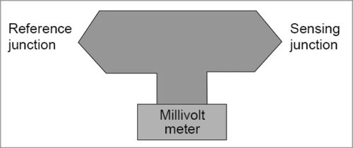
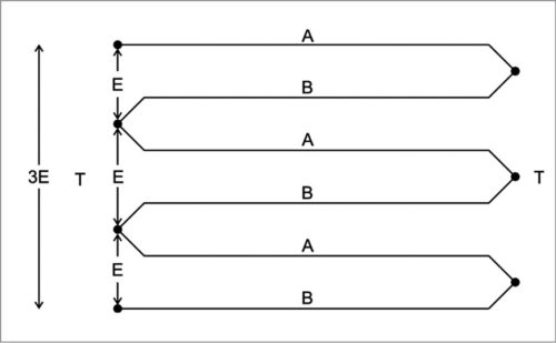
Fig. 14 shows some representative thermocouples. The responsivity of a single thermocouple is very low and therefore to increase the responsivity, several junctions are connected in series to form a thermopile (Fig. 13). Thermopiles are series combination of around 20-200 thermocouples. Spectral response of thermocouples and thermopiles extends into the far-infrared band up to 40µm. These are suitable for measurements over a large temperature range up to 1800K. However, thermocouples are less suitable for applications where smaller temperature differences need to be measured with great accuracy, such as 0-100oC measurements with 0.1oC accuracy. For such applications, thermistors and RTDs are more suitable.
Bolometers
Bolometers are the most popular type of thermal sensors. The sensing element in bolometers is a resistor with high temperature coefficient. While in photoconductors direct photon-electron interaction causes a change in the conductivity of the material, in bolometers the increased temperature and temperature coefficient of the element cause the resistance change.
Bolometers can be further categorised as metal bolometers, thermistor bolometers and low-temperature germanium bolometers.
Metal bolometers uses metals such as bismuth, nickel and platinum with temperature coefficient in the range of 0.3-0.5 per cent/°C. Thermistor bolometers are the most popular and find applications in burglar alarms, smoke sensors and other similar devices. Their sensor is a thermistor, which is an element made of manganese, cobalt and nickel-oxide.
Thermistors have high temperature coefficient of up to 5 per cent/°C. The temperature coefficient varies with temperature as 1/T2. Thermistors are classified as negative-temperature-coefficient (NTC) and positive-temperature-coefficient depending upon whether their temperature coefficient of resistance is negative or positive.
Pyroelectric sensors
Pyroelectric sensors are characterised by spontaneous electric polarisation, which is altered by temperature changes as light illuminates them. These are low-cost, high-sensitivity devices that are stable against temperature variations and electromagnetic interference. Pyroelectric sensors only respond to modulating light radiation and produce no output for a CW incident radiation.
Pyroelectric sensors operate in two modes: voltage and current. In voltage mode (Fig. 15), voltage generated across the entire pyroelectric crystal is detected. In current mode (Fig. 16), current flowing on and off the electrode on the exposed face of the crystal is detected. Voltage mode is more commonly used than current mode.
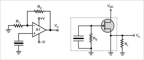
Voltage-mode pyroelectric sensors are generally integrated with a field-effect transistor. A shunt resistor (RS) in the range of 1010 to 1011 ohms is added to provide thermal stabilisation. External connections include a power supply and load resistor RL. The output voltage appears across RL. Modulation frequency in current-mode operation can be much higher than in voltage-mode operation. Hence it is much easier to separate the signal from the ambient temperature drift.
To be continued…
Dr Anil Kumar Maini was formerly a scientist and director of Laser Science and Technology Centre (DRDO)
Nakul Maini is a postgraduate in optical engineering from University of Bristol (UK), currently working as analyst with Ericsson

As a Citizen’s Science Researcher I am encouraged by the number of articles being provided by companies now designed to inform the general public about the health threats posed by unsecured embedded sensor networks and electronic devices on the Internet-of-things. In my community outreach efforts I’m finding growing interest in the security technology available for average families who may not be familiar with the science underlying IoT connectivity but are willing to study ways to protect themselves once they’re given tools that enable them to do so.