
Scientists have come up with a new device called shadow-effect energy generator (SEG), which makes use of the contrast in illumination to harvest energy under weak ambient light. This article covers the architecture and application of SEG in energy generation.
Shadows are everywhere, and not much engineering use has been found for these. In conventional photovoltaic or optoelectronic applications where a steady source of light is used to power devices, the presence of shadows is undesirable since it degrades the performance of devices. But scientists have come up with a new device called shadow-effect energy generator (SEG), which makes use of the contrast in illumination that arises on the device from shadow castings to generate a direct current at 1.2V.

This device is capable of harvesting energy from illumination contrast arising under weak ambient light. Without any optimisation, SEG has a power density of 0.14 microwatt/square cm under indoor conditions of 0.001 suns where shadows are persistent.
It performs 200 per cent better than commercial silicon solar cells under the effect of shadows.
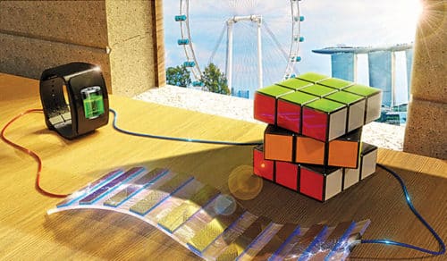
The cost of components used to make SEG is around thirty to fifty dollars per square metre, compared with the hundreds of dollars used to make commercial solar panels. An SEG device with multiple generators in operation is shown in Fig. 1.
Architecture
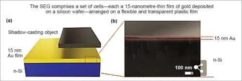
Inside the shadow-effect energy generator, there is a set of silicon wafers that are arranged in a flexible and transparent plastic film. Each silicon wafer is deposited with an ultra-thin gold coating that is only 15nm thick (for reference, human DNA is about 2.5nm thick). When light meets silicon, photons or light particles knock electrons free from their atoms, which creates an energy flow.
This is exactly the same process that a solar cell follows, but the gold layer is the true standout. With the gold coating, the device brings a stronger electric current when it is partially obscured in a shadow. As the agitated electrons jump from the silicon to the gold layer, the metal’s voltage increases when there is a difference between the light and dark portions. The optimum surface area for electricity generation is when half of the SEG is illuminated, and the other half is in the shadow as this gives enough area for charge generation and collection, respectively.
Plasmonics for photovoltaics
Plasmonics is the name given in 2000 to the discipline for exploiting resonant interaction obtained under certain conditions between electromagnetic radiation (light in particular) and free electrons at the interface between metal and dielectric material like air or glass. This interaction generates electron density waves called plasmons or surface plasmons. One of the most promising ways to enhance the localised light absorption and improve the efficiency of thin solar wafers is to use plasmonic structure. Plasmons are embedded metal nanostructures that can localise incident light on a sub-micrometric scale, enabling light concentration and trapping.
Conventionally, photovoltaic absorbers must be optically thick to allow near-complete light absorption and photocarrier current collection. Fig. 2 shows the standard AM1.5 solar spectrum together with a graph that illustrates what fraction of the solar spectrum is absorbed on a single pass through a 2µm thick crystalline silicon film.
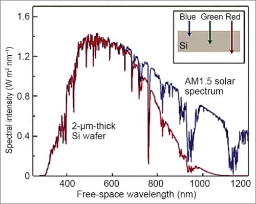
Clearly, a large fraction of the solar spectrum, in particular in the intense 600nm to 1100nm spectral range, is poorly absorbed. This is the reason that conventional wafer-based crystalline silicon solar cells have a much larger thickness, typically 180µm to 300µm. Around forty per cent of the cost of a solar module made from crystalline silicon is the cost of the silicon wafers.
The cost can be reduced if solar cells of reduced thickness deposited on a chip substrate like plastics are used. A major limitation in all thin-film solar cell technologies is that their absorbance of near-bandgap is ineffective, in particular for the indirect-bandgap semiconductor silicon. Therefore structuring the solar cell suitably so that light is trapped inside, in order to increase absorption, is very important. This can be quite effectively done by embedding gold nanoparticles (NPs) on a silicon wafer.
Plasmonic structures can offer at least three ways of reducing the physical thickness of the photovoltaic absorber layer while keeping their optical thickness constant, as shown in Fig. 3.
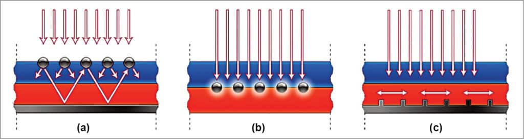
First, when a gold NP is placed close to the silicon wafer, the light will scatter with an angular spread in the silicon, which effectively increases the optical path length (Fig. 3(a)). Moreover, the light scattered at an angle beyond the critical angle for reflection, which is sixteen degrees for the silicon/air interphase, will remain trapped in the cell.
Second, gold NPs can be used as sub-wavelength antennas in which the plasmonic near field is coupled with the silicon wafer, increasing its effective absorption cross-section (Fig. 3(b)). Light is trapped by the excitation of localised surface plasmons in gold NPs embedded in the semiconductor. The excited particles’ near field causes the creation of electron-hole pairs in the semiconductor.
Third, a corrugated metallic film on the back surface of the thin silicon semiconductor absorber layer provided in SEG can convert sunlight into ‘surface plasmon polariton’ (SPP) modes, supported at the metal/semiconductor interphase (Fig. 3(c)). SPPs are infrared or visible frequency electromagnetic waves that travel along with a metal-dielectric or metal-air interface. SPP waveguide-coupled back reflector geometry contributes efficient trapping of light and roughly twenty-fold enhancement in the red to infrared solar spectrum.
If the SEG is provided with reflecting metal back contact, light reflected towards the surface will combine with the nanoparticles and partly reradiate into the wafer by the same scattering mechanism (Fig. 4). As a result, the incident light will pass several times through the silicon semiconductor film, increasing the effective path length.
The thickness of the n-silicon semiconductor in earlier SEG is about 170 to 180 micrometres. Using this advanced light trapping strategy along with a properly designed NP architecture, the wafer thickness can be dramatically reduced to around tenth of the aforesaid thickness, keeping solar cell efficiency at twenty per cent. Without a light-trapping technique, thin-film silicon chips would have about seven per cent efficiency. This will reduce the cost of the device greatly.
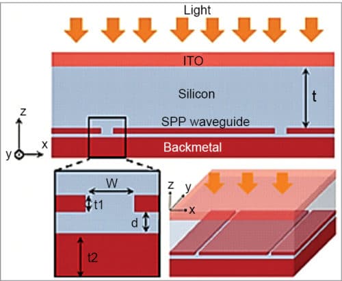
Thin-film crystalline silicon is formed at low temperature by plasma CVD with submicron grain size. After etching the pattern and providing reflectors, the thin film (~17 to 20µm) silicon wafer is fixed to the flexible substrate using epoxy-based adhesive.
Applications
With lower cost, simplicity, and stability, SEG offers a promising architecture to generate green energy from ambient conditions to power various electronic gadgets and as a part of smart sensor systems, especially in buildings. It can serve as a self-powered sensor for monitoring moving objects by tracking the movement of shadows.
When an object passes by the SEG, it casts an intermittent shadow on the device and triggers the sensor to record the presence and movement of the object. The harvested energy using eight of these generators in the presence of shadows at very low intensity (0.0025 suns) can drive a 1.2V electronic watch. Scientists are looking at ways to embed the small generators into clothing as a smart textile so that we can collect energy on the go.
Influence of gold nanoparticles
Plasmonic nanoparticles emerged recently as a possible solution to enhance solar cell efficiency. High losses of photons due to both incomplete absorptions of the solar spectrum and thermalisation are the main drawbacks that have been addressed to overcome limitations in photovoltaics efficiency.
Surface plasmon resonance (SPR) arises in metal nanoparticles (NP) as a collective oscillation of the surface electrons when subjected to the electric field associated with the incident light. SPR is the resonant oscillation of conduction electrons at the interface between negative and positive permittivity material stimulated by incident light.
Permittivity is a measure of the electric polarisability of a dielectric. Also, NPs should be smaller than the wavelength of the incident light, enabling them to polarise in order to achieve SPR.
The scattering and absorption of light depend on the polarisation of the NPs, which is a function of the size, refractive index, shape, density, and the surrounding medium. These parameters should be tuned in order to maximise the NPs’ light scattering relative to absorption. Scattering lower than fifty per cent may lead to heat dissipation and absorption suppression. This promotes the undesired reduction of photocurrent for solar cells having a high response in the blue region.
NPs used as a front electrode lead to an enhancement of the intrinsic layer absorption above 59 per cent in another light spectrum like the infrared region. Silicon does not absorb light very well. For this reason, more light needs to be scattered across the surface in order to increase the absorption.
It has been found that metal nanoparticles like gold NPs help scatter the incoming light across the surface of the silicon substrate. A common design is to deposit gold NPs on the top surface of the silicon wafer, as shown in Fig. 5.
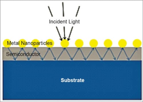
When light hits these gold NPs at their surface plasmon resonance, it gets scattered in many different directions. This allows light to travel along the silicon wafer and bounce between the substrate and NPs, enabling the solar cell to absorb more light. The concentrated near-field intensity induced by localised surface plasmon of the NPs promotes the optical absorption of the semiconductor.
The scattering cross-section of 15nm gold NPs embedded in silicon is many times (roughly thirty times) larger than its geometric cross-section. Therefore small surface coverage with these particles can highly scatter the incident light.
A simple and compatible process like thermal evaporation assisted by an electron beam to deposit gold NPs directly on the silicon wafer can be used. The layer thickness is controlled after opening the shutter of the system by the deposition time and a calibrated quartz crystal detector.
There is a decrease in transmittance as the gold NPs’ thickness increases, while the diffused light is enhanced for higher thickness. At 15nm thickness of gold NPs, the transmittance is about eighty to ninety per cent, and reflectance is about fifteen per cent.
Photocurrent under partial illumination
When one half of the gold surface is selectively illuminated and the other half is blocked from light, photocurrent flows. When the dark and bright zones are swapped in reverse mode, a photocurrent of equal magnitude but of an opposite polarity flows.
There is a directional electron flow on the surface that always flows from the bright to the dark zone. This indicates a change in surface potential induced by illumination.
On the other hand, when the entire surface is uniformly illuminated, the photocurrent and photovoltage are significantly low.
Effect of gold film thickness
There is a 33 per cent reduction in photocurrent upon increasing the gold film thickness from 15nm to 60nm. And there is more than a four-fold drop in photoresponse when the thickness is further increased to 300nm under same lighting condition using white light of ~18mW/sq cm. The photovoltage also gets reduced, as shown in the curve (Fig. 7).
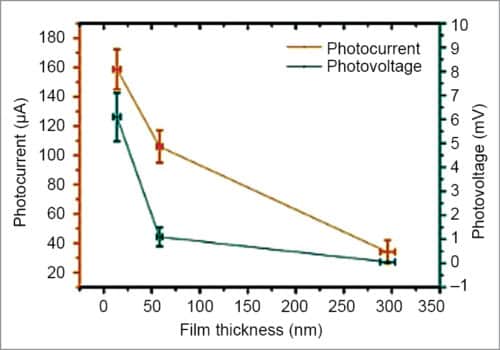
This is suggestive of the role of the underlying silicon substrate in driving photoresponse and the need for the gold film to be thin enough for the photons to reach the silicon interface.
Rathindra Nath Biswas is a 1964-batch chemical engineering graduate from Jadavpur University, Kolkata. He was awarded a certificate for designing Benzol Plant by Giprokoks, USSR, and Certificate of Honour by Indian Institute of Metals. He has published 35 research papers in various journals. He retired from service as head – MECON, Durgapur