


A solar cell is a sandwich of two different layers of silicon that have been specially treated or doped to let electricity flow through them in a particular way. This article covers the working principle, architecture, and uses of advanced multi-junction solar cells in achieving efficiency like never before.
Single-junction flat-plate terrestrial solar cells are fundamentally limited to about 25 per cent solar to electricity conversion efficiency. Scientists at the National Renewable Energy Laboratory (NREL), USA, have fabricated a solar cell that now holds the world record for the highest solar conversion efficiency of 47.1 per cent using a monolithic, series-connected, six-junction inverted metamorphic structure operated under the direct spectrum at 143 sun concentration. A variation of this structure achieves a one-sun global efficiency of 39.2 per cent. One sun is equivalent to 100mW/cm2 of irradiance.

Working principle of solar cell
A solar cell is a sandwich of two different layers of silicon that have been specially treated or doped to let electricity flow through them in a particular way (Fig. 1).
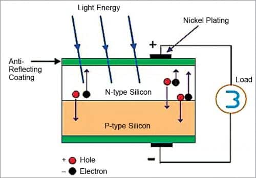
The lower layer is doped in such a way that it has very few electrons. It is called p-type or positive type. The upper layer is doped the opposite way to give it lots of electrons. It is called n-type or negative type. A barrier is created at the junction of the two layers, and no electrons can cross this barrier.
But something remarkable happens when the sun shines on the sandwich. Streams of energetic ‘light particles’ called photons enter the sandwich. They give up their energy to the atoms of semiconductors, which knocks electrons out of the lower p-type layer.

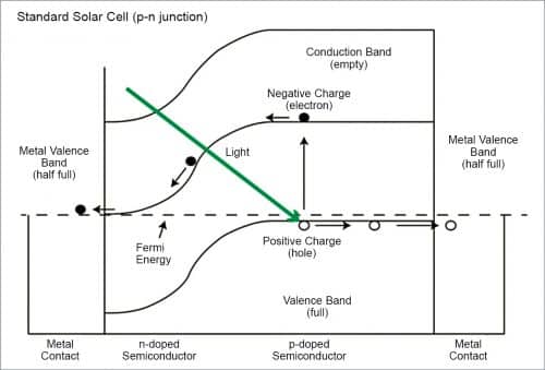
Usually, these electrons are in the valence band. The energy given to electrons by photons excites them into the conduction band, leaving behind an empty space called ‘hole.’ An electron from a neighbouring atom can move into this hole. The dislocated electrons jump across the barrier to the n-type layer above and flow out around the circuit to maintain the equilibrium, as shown in Fig. 2.
Band gap
The lower energy level of a semiconductor is called the ‘valence band,’ and the energy level at which an electron is considered free is called the ‘conduction band.’ A band gap is the energy difference in electron volts between the top of the valence band and the bottom of the conduction band. It represents the minimum energy that is required to excite an electron up to a state in the conduction band where it can participate in conduction.
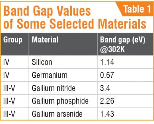
Semiconductor materials are nominally small band gap insulator. These materials can be doped with impurities that alter their electronic properties in a controllable way. An electric volt is the amount of kinetic energy gained or lost by a single electron accelerating from rest through an electrical potential difference of one volt in a vacuum. Band gap values of some selected materials are shown in Table 1.
Loss mechanism in solar cells
Multi-junction solar cells with concentrator can have over seventy per cent theoretical efficiency. But various mechanisms given below result in a chasm between efficiencies promised from theoretical calculations and those reached in practice.
Reflection loss. The reflection loss occurs from the top surface of the cells. Photons striking the top surface are reflected due to high reflectivity in the UV and visible regions, resulting in the absorption of a small portion of incident light leading to poor efficiency. These losses account for about thirty per cent. To reduce the reflection loss, a common approach is the use of an antireflective coating (ARC) of about 60nm thickness in the form of inverted pyramids by etching the surface with acid.
Recombination loss. Photon incident on the solar cells generates electron-hole pairs called carriers. These carriers need to be separated before they recombine with the emission of energy. Recombination causes loss of carriers and affects the performance of the cell.
Series resistance loss. Power losses in the solar cell take place due to a combination of resistance in series. Series resistance losses contribute to around twenty per cent of the total input power. But these losses increase tremendously when solar cells are operated at high intensities using lenses or mirrors.
Heavily doping of the semiconductor region helps in generating surface fields, which reduce the recombination at the metal-semiconductor contact. This is called tunnelling because the carriers can just tunnel through the junction. Other measures like the use of high conductivity substrate material, optimising the junction depth, increasing the number of fingers, using silver or gold, or electroplating metal contacts with these precious metals reduce the resistance.
Thermal loss. A major portion of the loss in a solar cell is due to heat. Light absorbed by solar cells has excess energy than that required for the generation of carriers. This excess energy is released in the form of heat. Proper cooling arrangements are used to maintain the temperature within limits.
Spectral mismatch loss. Single-junction solar cells suffer from intrinsic efficiency losses due to spectral mismatch of various wavelengths of light. The inability to absorb photons with an energy lower than the band gap and relaxation losses of the excess energy of absorbed high energy photons make up about 65 per cent of the total energy loss in a single-junction solar cell. The use of multiple p-n junctions made of different semiconducting materials with matching band gap energy allows the absorbance of a broader range of wavelengths, thereby improving the cell’s sunlight to electrical energy conversion efficiency.
Multi-junction (MJ) solar cells
Multi-junction or stacked solar cells are currently the most efficient cells available that convert up to 45 per cent of the solar energy they absorb into electricity under concentrated sunlight. The high efficiency of these cells stems from their ability to utilise a broad range of the solar spectrum from 300nm to beyond 1800nm, while controlling the spectrum incident on each subcell to minimise the energy loss of photogenerated carriers as these thermalise to the band’s edges.
MJ solar cells are primarily constructed of III-V semiconductor materials. These semiconductor materials are from groups III and V of the periodic table of chemical elements.
Theoretically, an infinite number of junctions would have a limiting efficiency of 86.8 per cent under highly concentrated light, implying that more junctions increase efficiency. The maximum theoretical efficiency is 37, 50, 56, and 72 per cent for 1, 2, 3, and 36 p-n junctions, respectively.
As the cell approaches the limit of efficiency, the increase in cost and complexity grows rapidly. MJ solar cells are solar cells with multiple p-n junctions made by stacking different semiconductors with varying band gaps on top of one another.
Each material’s p-n junction will produce an electric current in response to different wavelengths of light, improving the cell’s sunlight to electric energy conversion efficiency. However, these cells are ten times more costly than less efficient thin-film silicon solar cells, which have an efficiency of about 20 to 25 per cent. Their higher price-to-performance ratio has limited their use in aerospace.
One can’t merely stack different solar cells on top of each other because the different materials are structurally incompatible and so charges can’t pass through them. To solve this problem, in current multi-junction solar cells, heavily doped metals are used to create a tunnel junction between the various layers—adding significant complexity, which increases the cost. The tunnel junction enables electrical connectivity by acting as a metal to-metal connection.
There is another technique under development by North Carolina State University in the USA, in which the existing metal contacts of the individual cells are covered with indium films. The indium films bond to themselves easily at room temperature under low pressure.
This method, if commercialised, would benefit the manufacturers who make multiple types of single-junction solar cells using say silicon, III-V materials, etc. Single junction solar cells made of two different materials can be mechanically stacked and electrically connected to produce MJ solar cells, as shown in Fig. 3.

This technique enables the manufacturers to use the existing plant and equipment and simply tweak their existing products slightly to produce more efficient multi-junction solar cells rather than having to create new products, resulting in considerable cost reduction.
How a multi-junction cell operates?
The behaviour of MJ solar cells is inherently different than that of conventional single-junction (SJ) solar cells. The internal series connection of several junctions with different band gaps makes these devices more sensitive to incident spectral irradiance. The energy needed to excite the electron across the junction or gap is the band gap energy (in eV).
Only certain frequencies of light that have energy equal to or higher than eV of a particular material can excite the electrons across the junction. However, the light that has lower energy will pass through.
The size of the band gap dictates the energy generated by exciting an electron. A smaller band gap will result in lower energy. Therefore there is a balance between having a small band gap that will utilise many photons and having a large band gap that will utilise fewer photons and yet generate optimum energy. The optimum band gap is 1.4eV, and a single junction solar cell with this eV has a theoretical efficiency limit of 31 per cent approximately.
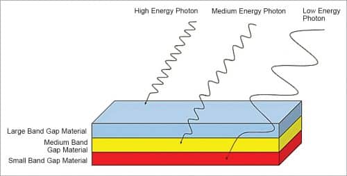
The actual efficiency can be greatly improved with the addition of multiple p-n junctions with multiple band gaps and working in tandem. With the various band gaps, the higher energy photons can be better utilised by materials with large band gaps, while the lower energy photons can be utilised by those with smaller band gaps. This is the basic principle of operation of a multi-junction cell. A multi-junction cell layers the materials in descending order, with the largest band gaps on top and the smallest on bottom, which creates a ‘photon sorting’ effect.
Photons with high energy are absorbed by the top layer more efficiently than if they were absorbed first by the bottom layer. Other spectrums of light having middle energy photons are transmitted through the top layer and absorbed by the middle layer photovoltaics, while the lower energy photons continue to pass through and are ultimately captured by the lowest layer of the solar cell. By deploying multiple junctions, the light that would otherwise have been wasted as heat can now be converted into electricity (refer Fig. 4).
Materials used in multi-junction solar cells
The multi-junction cells leverage the properties of semiconductors comprising elements in the III and V columns of the periodic table. The most common material used is gallium arsenide (GaAs), as it has a band gap of 1.43eV, which is extremely close to the optimal band gap range. It has six times higher electron mobility than silicon, which allows faster operation. It is used in conjunction with indium gallium phosphide (InGaP) and germanium (Ge) layer, with bandgaps of 1.85eV and 0.67eV, respectively.
InGaP utilises high energy photons, while Ge utilises much lower energy photons, and GaAs utilises those in between. Increasing the number of junctions increases the efficiency of the cell. But the numbers can’t be increased as per will. There is an upper limit.
The increase in film thickness decreases the transmittance of light, and photons may not make it to the bottom layers of the cell. The inverse also has a limit. If the semiconductor films are too thin, these will transmit too much light and will not absorb all the photons.
In MJ solar cell, lattice structures of adjacent layers have a bearing on its efficiency. Layers can either be lattice-matched or lattice-mismatched, as shown in Figs. 5 (a) and 5 (b), respectively.
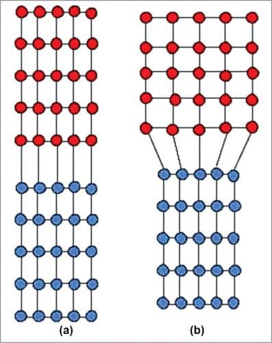
The mismatch of the lattices produces a lower band gap as opposed to that of the matched lattices. With the addition of an active Ge subcell, upright three-junction solar cells with lattice-matched InGaP/InGaAs/Ge designs have achieved more than thirty per cent efficiency under one sun illumination and 41.6 per cent efficiency under 364 suns.
The Ge subcell makes incomplete use of higher energy photons as carriers. This problem can be addressed by dividing the solar spectrum more finely using cells with five, six, or even more junctions. The subcell bandgaps needed for these MJ cell designs can be accessed easily with III-V materials that are not all at the same lattice constant.
However, such lattice-mismatched or metamorphic materials typically have crystal dislocations that act as recombination centres. Special techniques during manufacturing are used to reduce crystal imperfections.
For terrestrial applications, the high cost of these semiconductor substrates may be offset by using concentrating optics, primarily using Fresnel lenses. Fresnel lenses are shaped like a dartboard, with concentric rings of prisms around a lens that is a magnifying glass and placed on top of a solar cell, as shown in Fig. 6.
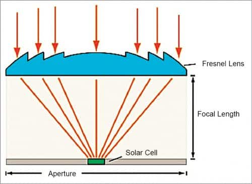
These focus scattered light to a tight beam. The concentrating optics increases the amount of light incident on the solar cell, thus leading to more power production. Concentrating optics allows individual cells to be quite small—at times as small as the size of a pencil tip. Therefore this technique allows hundreds of solar cells to be grown in a single batch. This decreases the number of solar cells needed and hence cost.
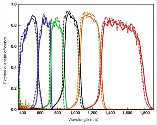
Architecture of multi-junction solar cell
The architecture of an MJ solar cell and a graph showing its utilisation of the solar spectrum is shown in Fig. 7.
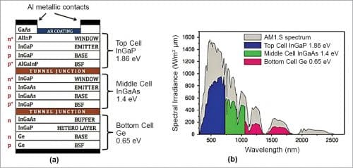
The function of an emitter window layer is to render passivity in the emitter surface. In any solar cell, a high surface recombination velocity will reduce the photoresponse of the solar cell, mostly in the blue portion of the solar radiation spectrum. AlInP is generally used as a window layer. It provides reasonable confinement in the emitter of an n-on-p device. It upgrades the blue response and fill factor of the solar cell.
Tunnel junctions act like diodes in reverse polarity to the original configuration in the stack of subcells. These provide better optical, electrical, and mechanical matching between the subcell layers.
The tunnel junction between subcell layers provides a low resistance connection between the p-type back layer of a subcell and the n-type window layer of the subcell beneath it. If tunnel junction is not provided, this p-n junction could produce a photovoltage that could roughly negate photovoltage generated by the top cell.
After every diode layer, a high quality and highly transparent back surface field passivation layer (BSF), typically with a higher band gap than that of the next sublayer cell, is introduced to prevent carrier recombination by repelling them back to the p-n junction without increasing the series resistance of the device. Thus, it increases the efficiency of solar cells. The high recombination velocity at the interface otherwise would affect photoresponse, particularly the red colour and open-circuit voltage to a great extent. AlGaInP and AlInP are popularly used as BSF layers.
Production
Multi-junction III-V cells are assembled in an epitaxial monolithic stack with subcells connected in series through tunnel junctions. Constructing a multi-junction cell in monolithic stack results in material constraints, and fabricating such devices is facilitated if the individual layers of subcells have compatible atomic lattice positions and are lattice-matched.
This is why Ge, which is lattice-matched to some III-V alloys, is traditionally used as substrate and narrow band gap cell in MJs. Lattice matching limitations can be overcome using wafer bonding or metamorphic buffer layers.
The tunnel-junction layer is constructed by the interphase of highly doped p++ and n++ layers. The interaction of these layers results in a spatially narrow space-charge region, which allows current to flow between subcells. High band gap layers, known as window layers and back surface fields can be added to passivate surface states at the interface between subcell and tunnel junction.
If the subcells are connected in series, the subcell that conducts the smallest current limits the maximum current that can flow through the device. Therefore a considerable effort is placed on tuning the current of the subcells. Luminescent coupling between subcells can relax some of the current matching design requirements.
MJ III-V solar cells are fabricated commercially in large metal-organic chemical vapour deposition (MOCVD) reactors. Layers can be grown from compounds of Ga and arsine in the hydrogen carrier gas and using dopants such as hydrogen selenide, silane and diethyl zinc.
Advanced MJ solar cells with 47.1 per cent efficiency
This year, in 2020, a group of scientists of NREL, USA, developed a six junction III-V solar cells with a 47.1 per cent conversion efficiency rate under 143 sun concentration and 39.2 per cent efficiency under one sun illumination. The device contains about 140 total layers of various III-V materials, but three times narrower than a human hair.
The new solar cells use a monolithic, series-connected, six-junction inverted metamorphic structure operated under the direct spectrum of the sun. Nearly optimal band gaps for six junctions were fabricated. During fabrication, it was ensured to minimise threading dislocations in lattice-mismatched III-V semiconductors and prevent phase segregation.
Three strategies have been adopted to make these advanced MJ solar cells with extraordinary high efficiency, as shown in Fig. 8, and their solar spectrum utilisation is shown in Fig. 9.
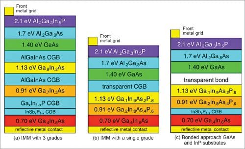
The scientists also developed metamorphic grades from the GaAs to the InP lattice constant, which are transparent to sub-GaAs band gap light. The inverted metamorphic multijunction (IMM) with six junctions demonstrated about fifty per cent efficiency under 1500 suns.
Rathindra Nath Biswas is a 1964-batch chemical engineering graduate from Jadavpur University, Kolkata. He was awarded a certificate for designing Benzol Plant by Giprokoks, USSR, and Certificate of Honour by Indian Institute of Metals. He has published 35 research papers in various journals. He retired from service as head – MECON, Durgapur
