


Researchers from India and China have harnessed MXenes as Schottky gates to optimise GaN transistors, reducing power consumption and voltage limitations.
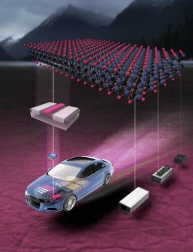
Computers are intricate systems of electronic switches processing digital information. Semiconductor technology shrinks and speeds up these switches. Gallium nitride, a semiconducting material, offers even more speed due to the rapid movement of charge carriers like electrons. Gallium Nitride (GaN) is valuable in high-frequency and high-power applications such as mobile chargers, 5G stations, radar, and satellites. Optimising High Electron Mobility Transistors (HEMTs), which utilise GaN, requires efficient electrical connections called Schottky gates. However, these gates often suffer from high leakage currents, power consumption and voltage limitations.

Chuanju Wang from Xiaohang Li’s team and Xiangming Xu from Husam Alshareef’s team and their co-workers and colleagues from India and China have demonstrated that the drawbacks can be reduced by creating the Schottky gate using MXenes. MXenes are a material consisting of ultra-thin two-dimensional layers of transition metal carbides, nitrides, or carbonitrides, which exhibit metallic properties.
Conventional metals have conventionally been used as electrical contacts to GaN, but their chemical interactions with GaN can result in defects that trap electrical charge and restrict gate controllability. Traditional metal gate contact materials are typically deposited using electron-beam evaporation and sputtering, forming a direct chemical bond with the semiconductor substrate. However, their research demonstrates that using a two-dimensional MXene material establishes a van der Waals contact with the semiconductor substrate, effectively mitigating interface traps and fixed charges.
Utilising ultraclean films of MXene Ti3C2Tx, the team engineered a GaN HEMT featuring a gate contact. Remarkably, their device demonstrated an extremely low off-state current of only 10^-7 milliamps per millimetre, a staggering six-order magnitude improvement compared to devices incorporating the conventional nickel-gold contact. This signifies that the current when the HEMT is in the “off” state is approximately 10^13 times smaller than in the “on” state.
Expanding the application of MXenes as Schottky-gate contact materials, the team aims to utilise them in various types of transistors, including Ga2O3, In2O3, NiO, and AlN. This step involves exploring the potential of MXenes in enabling improved performance and functionality in these transistor devices.
Reference:
Chuanju Wang et al, Ti3C2Tx MXene van der Waals Gate Contact for GaN High Electron Mobility Transistors, Advanced Materials (2023). DOI: 10.1002/adma.202211738