


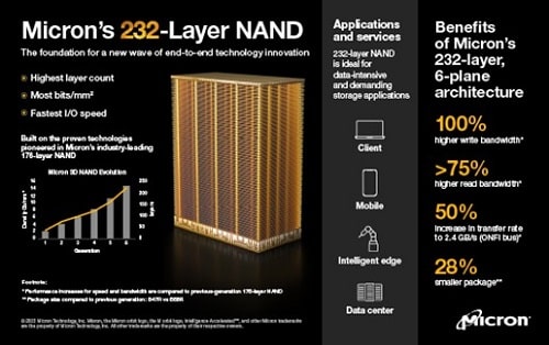
Micron Technology has announced the release of a high-density NAND with 232-layers. The NAND offers a fast NAND I/O speed of 2.4GB/s .The higher number of layers enables the storage device to offer higher energy efficiency and the industry’s highest areal density and delivers up to 100% higher write bandwidth and more than 75% higher read bandwidth per die than the prior generation. The storage device features highest number of plane per die of any TLC flash3 and features independent read capability in each plane. Furthermore, Micron’s 232-layer NAND is the first in production to enable NV-LPDDR4, thus making it suitable for use in application in the data center and at the intelligent edge nodes.
“Micron’s 232-layer NAND is a watershed moment for storage innovation as first proof of the capability to scale 3D NAND to more than 200 layers in production,” said Scott DeBoer, executive vice president of technology and products at Micron. “This groundbreaking technology required extensive innovation, including advanced process capabilities to create high aspect ratio structures, novel materials advancements and leading-edge design enhancements that build on our market-leading 176-layer NAND technology.”

In today’s data driven world, the need for higher density storage devices is the need of the hour and to meet the growing demand, Micron Technologies have introduced the 232-layer NAND. In addition, 232-layer NAND introduces the world’s first six-plane TLC production NAND.3 It has the most planes per die of any TLC flash3 and features independent read capability in each plane. The combination of high I/O speed, read and write latency, and Micron’s six-plane architecture provides best-in-class data transfers in many configurations. This structure ensures fewer collisions between write and read commands and drives system-level quality-of-service improvements.
According to the company, the higher number of layers reduces the size thus offering customers higher flexibility in their designs while enabling the highest TLC density per square millimeter ever produced (at 14.6 Gb/mm2). The NAND is shipped in a compact 11.5mm x 13.5mm package, which is 28% smaller package size than previous Micron generations.The interface is also backward compatible to support legacy controllers and systems. Micron’s 232-layer NAND technology can support advanced solutions and real-time services required in data center and automotive applications, as well as responsive, immersive experiences on mobile devices, consumer electronics and PCs, etc.
“Micron has sustained technology leadership with successive first-to-market advancements in NAND layer count that enable benefits like longer battery life and more compact storage for mobile devices, better performance in cloud computing, and faster training of AI models,” said Sumit Sadana, chief business officer at Micron. “Our 232-layer NAND is the new foundation and standard for end-to-end storage innovation underpinning digital transformation across industries.”