


The photonics bonder offers precision and adaptability in nano- and optoelectronics for product development and series production.
The advancing fields of nano- and optoelectronics are pivotal for future product innovations, requiring technological miniaturization and functional integration. Microassembly and assembly, and connection technology are vital for translating these technological advancements into commercially viable products. In this context, the precision and reproducibility of complex microsystems during manufacturing and assembly are essential for the quality and reliability of these products.
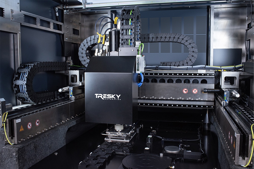
Tresky GmbH, a German DIE bonder specialist, has announced its photonics bonder, which is notable for its sub-micron placement accuracy. This bonder, featuring a granite base, is designed for precision, especially in nano- and optoelectronics. It offers a travel range of 500 x 700 mm and a bonding head with forces starting from 0.01 N, with options to increase the force range to 100 N, 300 N, or 500 N upon request.
The photonics bonder, built on a granite machine platform, is a placement system. It allows integration with all assembly and connection technologies that Tresky offers, including eutectic soldering or UV bonding. The modular bonder enables customization for specific customer needs and is suitable for prototyping, product development, and series production in nano- and optoelectronics. This adaptability facilitates a transition from prototype to production, allowing its use in both manual prototype production and series production. The photonics bonder can also accommodate optional bonding forces, making it suitable for hybrid bonding or sintering applications.
” As is standard for us, we use granite as a machine base so that the highest possible precision can be guaranteed for optical components such as VCSELs, lasers, photodiodes, IR sensors, and the development of quantum technologies. We configure the Photonics Bonder individually according to the customer’s requirements and thus adapt it specifically to the requirements, thanks to a high level of modularity. Therefore, the bonder can be reliably used in prototyping, product development, and series production of nano- and optoelectronics. Furthermore, the photonics bonder also supports bonding from wafers up to 12,” Daniel Schultze, managing director of Tresky GmbH, introduces the new bonder.
