This advancement paves the way for thinner and more efficient electronic devices, including wearables, signalling a new technological era.

In a development, scientists from Hunan University, the Chinese Academy of Sciences, and Wuhan University have successfully created monolayer transistors using unconventional two-dimensional (2D) semiconducting materials. This achievement marks a significant step forward in the field of electronics, as these materials hold great promise for the development of thinner and more efficient electronic devices, including wearables and smaller electronics.
2D semiconductors offer numerous advantages over traditional bulk materials, such as maintaining carrier mobility even when reduced in thickness. However, until now, the creation of monolayer transistors using these materials has been a rarity. Most attempts have focused on well-established 2D materials like graphene, tungsten diselenide, or molybdenum disulfide. The research showcases the successful fabrication of monolayer transistors using less common 2D semiconductors like black phosphorus (BP) and germanium arsenide (GeAs). These materials have been primarily used for multi-layer transistors due to challenges forming robust electrical contacts with delicate 2D substances.
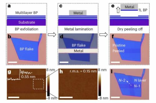
Lead author Wangying Li and her colleagues devised a van der Waals peeling technique to overcome these challenges. Laminating flat metals onto multilayer 2D channels could peel off the semiconducting layer at the top of the stack, leaving a monolayer transistor with 3D raised contacts. Their technique enabled the creation of homo-junctions and homo-superlattices based on various 2D semiconductors, including BP, GeAs, InSe, and GaSe. Remarkably, they achieved channel thinning while maintaining the necessary thickness in the contact region.
However, it’s worth noting that the carrier mobility of black phosphorus decreased as the body thickness reduced, resembling a conventional bulk semiconductor rather than a pure van der Waals semiconductor. Nevertheless, this discovery opens up exciting possibilities for thinner and scalable transistors using less conventional 2D semiconductors previously considered unsuitable for these applications.
The researchers believe their technique could have broader implications for other unstable monolayer materials, such as organic and perovskite monolayers, previously deemed non-conductive or of poor intrinsic quality due to inadequate metal-to-monolayer contact. This breakthrough brings us closer to creating advanced electronic devices that are thinner, more efficient, and based on a wider range of materials than ever before.


