


Despite the highly miniaturised size, the ultrasound detector is based on silicon technology rather than piezolectric technology that enables super-resolution imaging
Piezoelectric detectors have been commonly used to achieve good quality imaging resolution from ultrasound waves since the discovery of ultrasound imaging in the 1950s, converting pressure from ultrasound waves into electric voltage.

Reduced size of the piezoelectric detector helps deliver higher imaging resolution and can offer smaller, densely packed one or two-dimensional ultrasound arrays with an improved ability to distinguish features of a material. However, further reducing the size significantly affects their sensitivity, making them unusable for practical application.
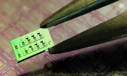
By leveraging silicon photonics technology (widely used to miniaturise optical components and densely pack them on the small surface of a silicon chip), researchers at the Technical University of Munich (TUM) and Helmholtz Zentrum München have now developed a much smaller ultrasound detector that has a size 100 times smaller than an average human hair, allowing to visualise features that were not previously possible and leading to what is known as super-resolution imaging.
Monitoring Light Intensity
While silicon does not exhibit any piezoelectricity, it can store light in dimensions smaller than the optical wavelength, which has been widely used for developing miniaturised photonic circuits.
The ultrasound detector: the silicon waveguide-etalon detector or SWED monitors changes in light intensity propagating through the miniaturised photonic circuits, instead of recording voltage from piezoelectric crystals.
“This is the first time that a detector smaller than the size of a blood cell is used to detect ultrasound using the silicon photonics technology”, says Rami Shnaiderman, developer of SWED. “If a piezoelectric detector was miniaturized to the scale of SWED, it would be 100 million times less sensitive.”
The SWED is about half a micron (0.0005 millimetres) in size (approximately 10,000 times smaller than the smallest piezoelectric detectors employed in clinical imaging applications.) The SWED is also up to 200 times smaller than the ultrasound wavelength employed, which leads to visualising features that are smaller than one micrometre for super-resolution imaging.
Future Mass Production
As the silicon platform can be considered to be robust, a large number of detectors can be mass-produced at a small fraction of the cost of piezoelectric detectors. This is important for developing several different detection applications based on ultrasound waves.
“We will continue to optimize every parameter of this technology – the sensitivity, the integration of SWED in large arrays, and its implementation in hand-held devices and endoscopes”, adds Shnaiderman.
“The detector was originally developed to propel the performance of optoacoustic imaging, which is a major focus of our research at TUM and Helmholtz Zentrum München. However, we now foresee applications in a broader field of sensing and imaging”, says Prof. Vasilis Ntziachristos, head of the Chair of Biological Imaging and director of the Institute for Biological and Medical Imaging at Helmholtz Zentrum München.
Besides aiming for applications in clinical diagnostics and biomedical research, the researchers are hopeful that industrial applications may also benefit from the new technology.