


(Credit: Nature electronics, A*STAR’s Institute of Materials Research and Engineering, Hong Kuan Ng et. al.)
Two-dimensional semiconductors usually have a unique property, that allows the thickness of the semiconductor to be mere atoms thick, this property has the potential to minimise the persistent issue of short channel effects, which remain like a thorn in the advanced silicon-based transistors, which often leads to turning on of a transistor prematurely. In spite of the massive potential of 2D semiconductors to replace the typical semiconducting materials like silicon, there’s one big issue with them, the low carrier mobility of 2D semiconductors at room temperature, which is usually caused by the scattering between electrons and phonons.
Carrier mobility measures how quickly a carrier, typically a hole or an electron can move through an electric field in a material, for example, if there’s a lot of traffic or bad roads, the amount of time and energy expenditure for commuting to two places can rise significantly. Similarly, the time and energy required for a hole or an electron to move to determine whether a material can be used as a semiconductor for electronic devices. High carrier mobility is essential to reduce power consumption in integrated circuits hence lowering the power dissipation as a whole, which in turn helps prolong the shelf life of electronic devices while also lowering the running costs.
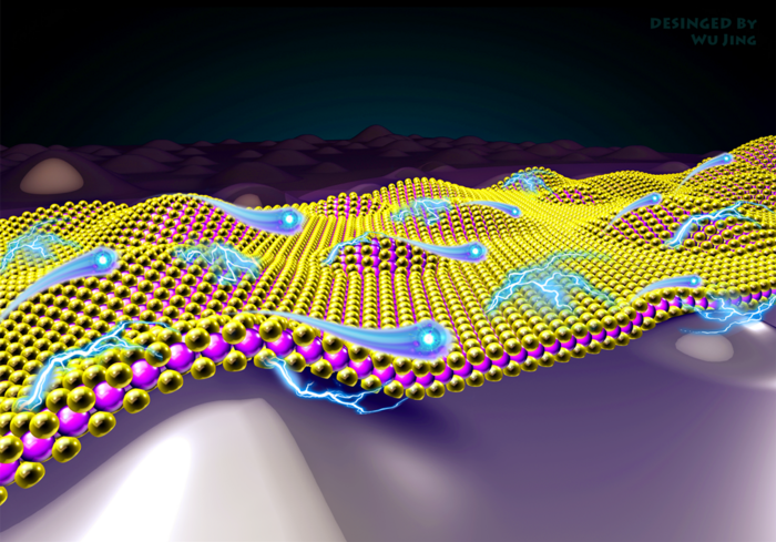
To tackle this issue, a group of researchers from the Agency for Science, Technology and Research’s (A*STAR) Institute of Materials Research and Engineering (IMRE), Fudan University, National University of Singapore and The Hong Kong Polytechnic University have come up with an innovative solution that introducing ripples, or placing the 2D material on a bulged substrate can improve and enhance the carrier mobility at room temperature by almost two times. The bulges help create ripples that distort the lattice structure, which moves one or more atoms from their original position in an ideal structure.
“Our approach is simple and cost-effective, demonstrating lattice engineering as an effective strategy to create high-performance room-temperature electronics and thermoelectric devices for future electronics,” said Dr Wu Jing, Scientist at A*STAR’s IMRE.
“We further reveal the underlying mechanism that the improved carrier mobility is due to the suppressed electron-phonon scattering and increased intrinsic dielectric constant induced by the rippled structures in the 2D semiconductor. Both of them play synergistic effects to boost the intrinsic carrier mobility,” said Dr Yang Ming, Assistant Professor at the Department of Applied Physics, The Hong Kong Polytechnic University.
The study can be found here.
