


Researchers at Tokyo Metropolitan University have developed nanostructures with junctions of transition metal dichalcogenides for creating integrated circuits with ultra-low power consumption tunnel field-effect transistors.
Field-effect transistors (FETs) are a crucial building block of nearly every digital circuit. FETs regulate current by voltage and are a fundamental part of digital circuits. Metal oxide semiconductor FETs (or MOSFETs) dominate, but the need for smaller and lower power devices has sparked interest in tunneling FETs (TFETs) that rely on quantum tunneling. TFETs are a potential alternative to FETs, using less energy. However, it is still an evolving field that requires further development.

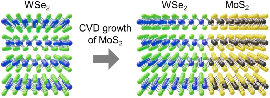
Researchers at Tokyo Metropolitan University have built nanostructures of transition metal dichalcogenides with junctions by growing multi-layered molybdenum disulfide from niobium-doped shards, creating planar heterostructures. These can produce ultra-low power consumption tunnel field-effect transistors for integrated circuits.
The team creates Transition metal dichalcogenides (TMDC) nanostructures for TFETs. TMDCs are suitable for TFETs due to the presence of transition metals and group 16 elements. They linked single-atom-thick TMDC sheets over longer distances recently. The researchers used CVD to grow multi-layered TMDCs from crystalline planes on a substrate, forming in-plane junctions. Previous attempts focused on monolayers but couldn’t create the high electron concentrations needed for TFETs.
Having established their method’s effectiveness with molybdenum disulfide grown from tungsten diselenide, the researchers shifted their focus to niobium-doped molybdenum disulfide, which is a p-type semiconductor. Cultivating multi-layered structures of undoped molybdenum disulfide, an n-type semiconductor, created a thick p-n junction between TMDCs with an exceptionally high carrier concentration. Additionally, they observed that the junction exhibited negative differential resistance (NDR), whereby increases in voltage resulted in progressively smaller increases in current. This is a crucial characteristic of tunneling and a significant initial advancement in enabling these nanomaterials to be utilized in TFETs.
The team’s approach is easily scalable to cover large areas, rendering it ideal for use in circuit manufacturing. This novel advancement is highly promising for contemporary electronics, as there is optimism that it will eventually be integrated into various applications.
Reference: “Multilayer In-Plane Heterostructures Based on Transition Metal Dichalcogenides for Advanced Electronics” by Hiroto Ogura, Seiya Kawasaki, Zheng Liu, Takahiko Endo, Mina Maruyama, Yanlin Gao, Yusuke Nakanishi, Hong En Lim, Kazuhiro Yanagi, Toshifumi Irisawa, Keiji Ueno, Susumu Okada, Kosuke Nagashio and Yasumitsu Miyata, 23 February 2023, ACS Nano. DOI: 10.1021/acsnano.2c11927