Researchers have developed a way to boost the efficiency of highly sensitive imaging sensor and also uses less energy than most such devices.

Security systems are being developed to meet various security applications. These systems need to be smart and precise at detection of any undesired events. For example, sensors that turn on as a reaction to light when the presence of an intruder is detected has become very common. This sensor is made up of a grid of pixels, each of which are reactive to light. Performance of such sensors are based on measurements of responsivity, and which parts of light they detect.
Researchers at Penn State University noted that most of these sensors are very inefficient, and are using far more electricity than what is required for such devices. Therefore, to make these sensors more effective, they replaced the traditional silicon complementary metal oxide semiconductor backbone with one made from molybdenum disulfide, a material that, like graphene, can be grown as a one atom thick sheet.
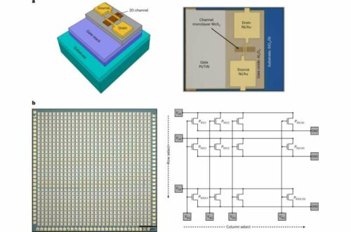
Researchers grew the molybdenum disulfide sheet on a sapphire base via vapor deposition. The finished product was shifted on a base of silicon dioxide that had already been wire etched. They then finished their product by etching additional wiring on the top.
The result of their work was a 30×30 grid, where each of the pixels was its own device—one that was not only capable of detecting light but could also be drained using an electrode that made it ready for use again after something had been sensed.
The device was recorded to be far more efficient than those currently in use, each pixel used less than a picojoule. They also found it very easy to reset. One shot of voltage across the array did the trick. On the other hand, the researchers found that it responded far slower to light than sensors currently in use. This suggests that it could be used as an all-purpose light sensor, but not as a fixture in a camera.
REFERENCES : Akhil Dodda et al, Active pixel sensor matrix based on monolayer MoS2 phototransistor array, Nature Materials (2022). DOI: 10.1038/s41563-022-01398-9


