


Silicon-based hybrid device that combines III-V tunnel FETs and conventional MOSFETs, paving the path for future energy-efficient electronics
Innovations at the transistor level over the past few years have been at the forefront of driving the electronics industry to new heights. The has always been to develop fast processing electronics components that are compact at the same time.
Metal-oxide-semiconductor field-effect transistors (MOSFETs) are the most conventional and widely used type of transistors. However, their high power inefficiency proves to be a limitation, which is due to their inability to reduce the voltage supply while simultaneously limiting the off-state leakage current.
The device known as a tunnel field-effect transistor (TFET) can overcome this limitation by taking advantage of quantum mechanical tunnelling instead of thermionic emission. TFETs, particularly those with a III-V heterostructure, require less than 60 mV of gate voltage swing to induce a variation of one order of magnitude in the drain current at ambient temperatures. Despite their lower power consumption, TFETs aren’t yet fast and energy-efficient like MOSFETs at higher drive voltages.
Relating to this, researchers at IBM Research Europe and École Polytechnique Fédérale de Lausanne (EPFL) have recently developed a silicon-based hybrid device that combines III-V tunnel FETs and conventional MOSFETs.
“We demonstrated the first hybrid technology platform combining III-V tunnel FETs and MOSFETs with a scalable process and suitable for large-scale semiconductor manufacturing,” said Clarissa Convertino, researcher at École Polytechnique Fédérale de Lausanne. “Such low-power technology platform paves the way to future energy-efficient electronics, with the ultimate goal of reducing the carbon footprint of the ICT industry,” she said.
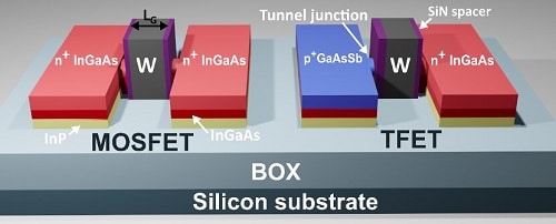
The new platform developed by Convertino and her colleagues exploits the synergies between tunnel FETs and MOSFETs, as it allows users to implement hybrid logic blocks tailored to the unique specifics of each type of device. In initial evaluations, the scaled III-V hybrid TFET-MOSFET device achieved a minimum subthreshold slope of 42 mV dec−1 for TFET devices and 62 mV dec−1 for MOSFET devices.
“Tunnel FETs provide lower leakage and good performance at low voltages levels, while MOSFETs are faster (at the same dimension and bias) and provide greater current drive,” Convertino explained. “The developed fabrication flow is identical for both devices except for a single masking and epitaxy step, opening up for manufacturing of truly hybrid logic blocks. Moreover, our tunnel FETs show record performance at the smallest gate length reported to our best knowledge,” she added.
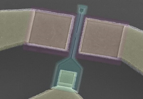
The remarkable performance achieved by the device is due to the introduction of a self-aligned source-replacement step. In their platform, the position of the GaAsSb source is determined by digital etching, a process that allows the removal of material in the nanometer range.
Convertino and her colleagues demonstrated the integration of an in-plane heterojunction tunnel FET in an advanced hybrid platform using replacement metal-gate and spacer technologies. In the future, this technology could enable the development of faster and more efficient electronic devices that combine the advantages associated with TFET and MOSFET transistors.
More details about the technology have been presented in a paper published in Nature Electronics.
