


A team of Researchers from Osaka University and collaborating partners invented a metal superlattice using conventional nanofabrication methods
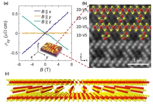
Researchers developed Vanadium-based superlattices using chemical vapor deposition, a popular nanofabrication technology in the industry. Anisotropic anomalous Hall effect (AHE), which is directionally concentrated charge buildup under in-plane magnetic field conditions (where the conventional Hall effect is not detected), is demonstrated by these magnetic semiconductors. This research assists in controlling the movement of electrons within the metal semiconductors to an extraordinarily high degree, which would result in the improvement of the operation of modern technology. This innovation will enhance the importance of microelectronics in mainstream technologies.
“Nanoscale hetero-dimensional superlattices are typically challenging to prepare but can exhibit valuable physical properties, such as anisotropic electrical conductivity. We developed a versatile means of preparing such structures, and in so doing we will inspire synthesis of a wide range of custom superstructures,” says Yung-Chang Lin, Study Senior Author, Osaka University. The AHE which are noticed at only extremely low temperatures but in the current study AHE was detected at a temperature above room temperature, up to at least the boiling point of water. This creates a hope of using AHE in everyday technologies if it’s produced at realistic temperatures.
Lin stated, “A key promise of nanotechnology is its provision of functionalities that you can’t get from bulk materials. Our demonstration of an unconventional anomalous Hall effect at room temperature and above opens up a wealth of possibilities for future semiconductor technology, all accessible by conventional nanofabrication processes.”
Utilizing materials with the same dimension that is sandwiched in 2D sheets, scientists can create nanostructured superlattices, that will result in regularly alternating layers of metal. This research will increase electronic device speed, lightning efficiency, and data storage density. Researchers aim to invent adaptable technology which exceeds the utility of natural materials by manipulating the nanoscale architecture of metals that are frequently used in industry.
Click here for the Published Research Paper