
These findings are likely to inspire researchers to create futuristic electronic devices, such as piezo FETs.
Researchers have developed a low contact-resistance metal-semiconductor interface with 2D monolayers for transistors. This can supposedly can improve device performance significantly.

These new 2D semiconducting monolayers (MgX X=S, Se, Te) with excellent charge carrier mobility have been proposed by scientists from the Indian Institute of Nanoscience and Technology (INST), an autonomous institute of the Department of Science and Technology (DST). The goal of this research is to find solutions to three fundamental problems in pure graphene: band gap opening by a non-invasive/non-destructive method, stacking dependent contact characteristics, and charge carrier concentration tunability. This research can be applied to electrical and spintronic devices made of graphene.
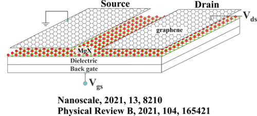
Professor Abir De Sarkar and his PhD students Manish Kumar Mohanta and Anu Arora investigated reduced contact resistance between semimetal graphene and MgX in a study published in Phys. Rev. B. They discovered complete non-resistive contact at the graphene-MgS interface, a rare and highly desired state for charge transport through the channel.
The proposed 2D monolayers are one-of-a-kind because they integrate flexibility, spintronics, and piezoelectric capabilities in a synergistic way, making them desirable for future self-powered nanoelectronics devices.

The discovery of graphene sparked a surge in interest in two-dimensional (2D) materials research. The absence of resistance in pristine graphene is a significant barrier to its use in electronics and switching devices. As a result, 2D semiconductors have developed over time to circumvent graphene’s restrictions.
The ability of these unique 2D monolayers to respond to vertical external electric fields can be used to store data in electronic devices. Because of the buckled structure and broken inversion symmetry, these monolayers have a strong out-of-plane piezoelectricity, which can be used to generate piezopotential by applying vertical strain. The piezopotential has the ability to control current flow, making MgTe monolayer-based devices self-powered!
Through the use of the proposed 2D monolayers, this research published in the journal Nanoscale expects considerable improvement in the field of spintronics and supports self-powered devices!