


Paper presented at the ISSCC 2021 shows how new adaptive back-biasing technique overcomes integration limits in chip design flows

CEA-Leti and Dolphin Design have developed an adaptive back-biasing (ABB) architecture for Fully Depleted Silicon on Insulator (FD-SOI) chips that can be seamlessly integrated into the digital design flow with industrial-grade qualification, overcoming integration drawbacks of existing ABB techniques.
FD-SOI is a technology that allows the biasing of the transistor’s body to act as a back gate. Unlike conventional bulk technology, FD-SOI enables a wide voltage range of body bias. This permits compensating for process, voltage and temperature (PVT) variations by controlling the threshold voltage. For example, in switch operations, when the switch is on, the body bias is changed to reduce the on-resistance by reducing threshold voltage and allowing more current to pass. That accelerates the circuit. In the off state, the body bias is changed to raise the off-resistance by increasing the threshold voltage, consequently reducing the leakage current. This shows that FD-SOI technology can be used either to accelerate the design or reduce the leakage power.
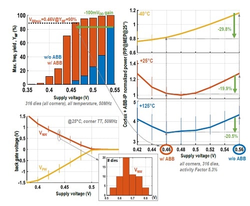
The new ABB technique also allows the application design to maintain a targeted operating frequency over a wide range of operating conditions such as temperature, manufacturing variability and supply voltage. The architecture enables a reduction in energy consumption of processors in 22nm FD-SOI technology by up to 30 per cent and increasing the operating frequency up to 450 per cent compared to a technique in which body biased technique is not used. It also improves the manufacturing yield.
“The ABB development is a breakthrough for FD-SOI technology because it shows the first-ever results depicting the enhancement in the circuit performance after using ABB and it will help increase performances and yields in FD-SOI designs,” said Gaël Pillonnet, a CEA-Leti scientist. “A 0.021 mm² PVT-Aware Digital-Flow-Compatible Adaptive Back-Biasing Regulator with Scalable Drivers Achieving 450% Frequency Boosting and 30% Power Reduction in 22nm FD-SOI Technology.”
“The performances of our ABB IP are state of the art and show the compensation of the variations across process-voltage-temperature (PVT) conditions on a representative number of samples, enabling the usage of this solution in industrial products,” said Andrea Bonzo, IP program manager at Dolphin Design. “Previous efforts in this technique have reported only limited numbers of chips that perform as intended. With our technique, a large number of chips are shown to work properly. ABB is versatile and can be used to drive a large digital area without any limitation for any FD-SOI technology.”
According to the paper, “the well-known adaptive back-biasing (ABB) technique has already shown its capability to reduce power consumption or/and maintain operating frequency by compensating VTH variability according to process corners and temperature. However, previously published ABB architectures provide a limited overview of how to integrate the ABB seamlessly in the digital design flow with industrial-grade qualification. We propose a reusable ABB-IP for any biased digital load, from 0.4-100 mm², with low-area and power overhead, e.g. 1.2 per cent @ 2 mm² and 0.4 per cent @ 10 mm², respectively.”
With this new architecture, the ABB area is relatively small compared to the application design, and in both area and power, it allows the application design to maintain its targeted speed (frequency) with relatively low overhead.
A paper regarding the above technique was presented at the ISSCC 2021.
