
It may now be possible to create a novel kind of semiconductor that is a few atoms thin and interacts with light in a unique way, thanks to a research collaboration between Penn State and the Massachusetts Institute of Technology (MIT).
Tin selenide (SnSe), a novel semiconductor material, will be helpful in the development of “photonics,” a new category of electronics that uses light’s photons to store, process, and transport data. The substance interacts strangely with light, which has a lot of promise for usage in electronics.
“It can be described as a material that has two different colors, meaning that depending on the orientation that you look at it, you will observe a different color,” said Wouter Mortelmans, a postdoctoral associate in the Department of Materials Science and Engineering at MIT, and lead author of the study. “This peculiar optical property could be very useful to compute, store, or transmit information using light.”
“We need a reliable way to make the material, to manufacture devices to spec, without worrying about random, natural variations,” said Rafael Jaramillo, Thomas Lord Associate Professor of Materials Science and Engineering at MIT and senior author of the study published in ACS Nano.
Epitaxy, a procedure that can be difficult for semiconductors made of atomically thin layers, is essential for producing such precise, defect-free materials. “Epitaxy can be imagined as similar to building with Legos, where the material of interest is broken up into small individual unit cells of either triangular or rectangular Lego bricks,” said Maria Hilse, assistant research professor, thin films-MBE, with the Penn State Materials Research Institute’s 2D Crystal Consortium (2DCC).

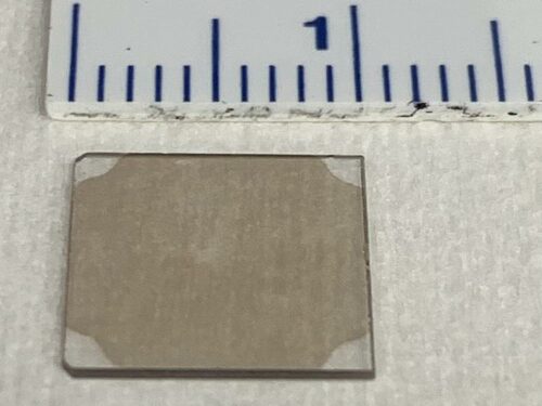
“The base is an ultra-clean host crystal substrate that allows for a certain shape of ‘Lego’ bricks to be put on it. We select this starting substrate plate, ideally, so that it fits perfectly with the crystal structure of the material we want to compose, i.e., our Lego bricks. In the case of SnSe, we would have a pool of rectangular-shaped Lego bricks that we want to assemble on a rectangular-shaped Lego base plate, which is an aluminum oxide (11-20) surface.”
Both academics and the general public stand to gain from the outcomes of this partnership, as shown in the study. “The study of epitaxy processes of 2D materials is a relatively young field with room for optimizations. With the new insights obtained in this work, we hope to further contribute to the advancement of epitaxy processes of 2D materials,” Mortelmans said.