
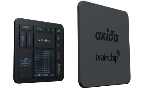
It comprises of 80 Neuromorphic Processing Units (NPU), providing 1.2 million virtual neurons and 10 billion virtual synapses
Increasing implementation of neuromorphic computing for various applications ranging from embedded vision and audio, automated driving to cybersecurity, and industrial IoT has led to rising demands for low-power artificial intelligence solutions.
And although IBM’s TrueNorth chip and Intel’s Loihi processor promise to resolve this issue, it is Brainchip’s Akida that has been the first to do so.
The Akida event domain neural processor is a next-generation AI IP with industry-leading performance.
Its configurability and scalability for continuous learning are ideal for Edge AI applications ranging from microwatts to milliwatts with a minimal memory footprint.
BrainChip IP allows incremental learning and high-speed inferencing in a wide variety of use cases with high throughput and unsurpassed performance-per-watt at low power.
BrainChip’s IP can be configured to perform convolutions (CNP) and fully connect (FNP) layers without requiring re-training. Weight bit-precision is programmable to optimise throughput or accuracy and each weight is stored locally in embedded SRAM inside each NPU.
The Akida chip comprises of 80 Neuromorphic Processing Units (NPU), providing 1.2 million virtual neurons and 10 billion virtual synapses. Each NPU comes with 100 KB of SRAM memory and is networked with its fellow NPUs into an on-chip mesh.
The entire neural networks can be placed into the fabric, removing the need to swap weights in and out of DRAM resulting in a reduction of power consumption while increasing throughput.
BrainChip’s IP fabric can be placed either in a parallelised manner for ultimate performance, or space-optimised to reduce silicon utilisation and further reduce power consumption.
Additionally, users can modify clock frequency to optimize performance and power consumption further.
Key Features
- On-chip mesh network interconnect
- Standard AXI 4.0 interface for on-chip communication
- Scalable nodes can be configured as event domain convolution neural processor or fully connected neural processor
- Uses 1-bit, 2-bit, or 4-bit (INT1, INT2, or INT4)
- Hardware-based event processing
- No CPU required
- External memory optional (SRAM or DDR)
- Configurable amounts of embedded memory and input buffers
- Integrated DMA and data-to-event converter
- Hardware support for on-chip learning
- Hardware support for lb, 2b or 4b hybrid quantised weights and
- Reduced power and minimised memory footprint
- Fully synthesisable RTL
Applications include smart appliances, sensors, robots/drones, automotive, audio and IIoT with use cases such as object detection, sound, facial and gesture recognition to packet inspection.