


With modern-day complex multi-chipset systems, power delivery designs are becoming challenging and more critical than ever. Power integrity analysis helps us understand the impact of each component and its parasitic value on the final performance of the CPU and helps in designing an optimised system for reliable operation.
Power distribution of a system plays a crucial role in its reliability and performance. Be it any system ranging from mobile phones to laptops to servers to national grids that are powering up the nation, key to reliable system operation is to deliver right amount of current to its different loads at right voltage levels.
Imagine 0.7V DC voltage at CPU (central processing unit) power input that is rated for 1-1.5V DC for stable operation or 350V AC at air-conditioner input that is rated for 230V AC. It is a known fact what happens next. Either the CPU hangs due to low voltage or the air-conditioner gets damaged due to high voltage at input.
The question that arises next is, how to ensure electrical reliability as a system designer? Power integrity is the answer. Power integrity ensures required voltage and currents are delivered from source to load within the system. Through power integrity analysis, one can understand voltage levels at various system loads under worst-case operating conditions, which is the ultimate test of electrical reliability. This article covers the power integrity analysis of electronic products only.
Advantages for the designer
Power integrity plays a significant role in the success and failure of electronic products. Following are the key advantages of performing thorough power integrity analysis of a system:
- Ensures design specifications are met at all system level components during worst-case operating conditions.
- Ensures the system is designed optimally, with right level of inbuilt safety margins, making it cost-effective.
- Stronger reliance on results based decisions rather than experience or thumb-rule based design.
- Allows system scalability and optimisations based on individual use cases. Need not rely on vendor guidelines based on generic designs that may not be cost-effective for a dedicated application.
Power delivery networks modelling
All electrical products, at basic level, can be reduced to electrical networks for modelling purpose. A power delivery network (PDN) comprises majorly a power source, single or multiple loads, and an interconnect path between the source and the load.
Fig. 1 shows a simplistic electric circuit equivalent of a PDN with load R connected to voltage source VS through path resistance RP. In a real system, such as a desktop or server motherboard, VS will be a voltage regulator (VR) powering up the CPU, which is modelled as R (load). The parasitic resistance of the layout/path on board connecting VR and CPU is modelled as Rp. This simple PDN model can be used to understand the importance of power integrity at preliminary stages of the design.
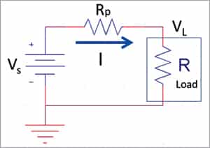
With increasing CPU current, which may be caused by increase in CPU clock frequency to execute a specific workload, voltage Vi at CPU input reduces due to higher voltage drop along the path or resistor Rp. Every electrical part, such as CPU, will have its maximum load demand Imax and minimum operating voltage Vmin required for stable operation defined in the part datasheet. Path resistance RP that ensures Vi >Vmin under all loading conditions is termed as target resistance (RTarget) of the design.
To model the design parasitic more accurately, series inductance of the layout is considered as well. With inductance involved, it’s no longer just resistance but impedance Zp of the layout that needs to be modelled. Layout Impedance Zp that ensures Vi >Vmin under all loading conditions within system frequency range of operation is termed as target impedance (ZTarget).
The main aim of power integrity analysis is to ensure parasitic impedance Zp of a system is less than ZTarget within system frequency range of operation. For any system, ZTarget will be determined based on its maximum load demand and maximum peak-to-peak noise that can be tolerated at input for reliable operation.
Fig. 2 shows a power delivery network of a CPU on a server or desktop motherboard system. It consists of a VR module, which is the main power source for CPU, followed by bulk capacitors at the output of the VR for limiting switching noise or ripple. There are motherboard capacitors placed close to the CPU, which are mostly multilayer ceramic capacitors (MLCC) that limit voltage falls during sudden inrush current demand by CPU.
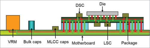
The CPU can be connected to the motherboard via socket mechanism or soldered down directly during assembly process. The printed circuit board that mounts the silicon die or CPU chip is called a package. On the package, there are land side caps (LSC) that are placed in the pin field region at the bottom side and die side caps (DSC) that are placed right next to the silicon die.
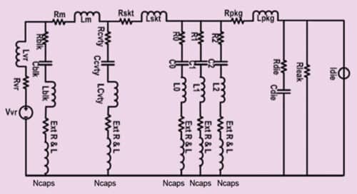
Fig. 3 shows an equivalent circuit model of the power delivery network, including realistic circuit models of each component, such as capacitors. Power integrity analysis helps us understand the impact of each component and its parasitic value on the final performance of the CPU and helps in designing an optimised system for reliable operation.
Power integrity analysis methodology
With understanding of the importance, lets discuss the process to be followed for complete PI analysis of any given system. We start with DC performance check of the system followed with AC or frequency domain analysis (FDA). At the end, we must perform the transient analysis that provides final go or no-go direction for the design and is the ultimate test for system reliability.
DC performance analysis
DC performance is #1 priority for any PDN. With DC analysis, we ensure design accounts for the following aspects:
- Steady state voltage drop at different system level components from respective voltage source.
- Current densities along the layout and its uniform distribution throughout.
- Maximum current flowing through individual vias on PCB.
- Power loss contribution of each individual board layer in case of multilayer PCB stack up.
Simulation setups for running DC analysis are fast and accurate. DC analysis is the first step before doing any kind of frequency domain or time domain analysis of the PDN.
Fig. 4 highlights a typical failure case of PDN that can be analysed and fixed through DC analysis. It shows a power layout (highlighted in green) from VR output to the load point. At load point, the voltage drops from 1V to 0.74V, which will render the chip non-functional. With such gaps identified, the layout can be optimised to reduce voltage drops and meet design specs for all system level components by ensuring path resistance is less than target resistance RTarget.
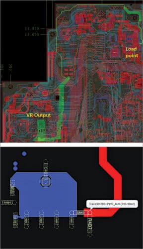
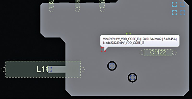
Fig. 5 highlights another failure case of a PDN with ~6.5A current flowing through single via in the design. Typical specification for a standard PCB design is maximum 2A current though via. If not accounted for, such high current would lead to via burn on PCB. Such issues can be fixed by either adding more vias in the regions with high current densities or changing via location/pattern in the layout.
Frequency domain analysis
Frequency domain analysis is helpful to understand PDN performance across a range of operational frequencies. With FDA, PDN impedance Z as a function of frequency is plotted and compared against target impedance ZTarget to ensure Z<ZTarget for system range of operational frequencies.
It is also helpful to understand power delivery performance sensitivity with different type of capacitors, such as bulk caps, motherboard caps, land side capacitor, etc (as shown in Fig. 2), number of capacitors and their respective placements. With optimal type, combination, and location of the capacitors studied and worked out through FDA, we can optimise and design a cost-effective power delivery solution, which is based on actual analysis of the system and not just thumb rules or generic vendor guidelines.

Fig. 6 displays an impedance profile of a typical PDN. The various crests and troughs in the impedance profile are result of resonance and anti-resonance between various series and parallel resistor-inductor-capacitor (RLC) combinations, as shown in Fig. 3. With reference to PDN shown in Fig. 3, the constant/flat impedance region in low frequency range of the profile is governed by effective resistance between the silicon die and VR source.
The first crest in the profile, around 100kHz frequency range, is dictated by parasitic inductance of the bulk capacitor. This is also referred to as third droop impedance. The trough close to 1MHz frequency range is governed by the bulk capacitor and other motherboard capacitors’ effective capacitance.
The second crest point in the plot is dictated by the motherboard parasitic inductance and the CPU-motherboard interconnect parasitic inductance. This point is referred to as second droop impedance. The trough following the second droop is governed by LSCs and the DSCs (die side caps).
The steep rise in the impedance leading to the third crest is dictated by package parasitic inductance and LSC/DSC parasitic inductance and is referred to as first droop impedance. The falling impedance in high frequency region >100MHz is governed by metal-insulated-metal (MIM) capacitances inside the silicon die.
It becomes extremely important to generate and understand the impedance profile of the system under test to run any kind of optimisation on the same. For example, addition or removal of bulk capacitor on motherboard will not have any impact on second droop impedance as it’s beyond the range of its frequency response. Package capacitors and package layout need to be optimised for reducing the same. Such design level understanding can only be achieved through system frequency domain analysis.
Transient analysis
Transient analysis is the ultimate test for system reliability. It helps in comparing the ‘final’ PDN performance with device level specifications defined in the datasheets. Also, the results generated can be correlated with actual validation results to estimate the overall simulation process accuracy. It involves generating a time-domain passive circuit model of the PDN under analysis.
With circuit model generated, proper voltage source (at VR location) and sink loads (at load devices) can be connected at respective nodes of the model to generate an overall circuit file. This circuit file can be simulated and analysed for results using any SPICE based circuit simulator, such as HSPICE, LTSPICE, etc. The key results generated are the time domain voltage profiles at the input of system level component under test, which then can be compared with the defined specifications.
Most crucial part of this process is generating an accurate circuit model of the PDN network. Any tool is as good as its input. In this case, SPICE simulator output results are as accurate as the circuit model used to generate the same.
Circuit model generation of the PDN under test is a two-way process. At first, frequency domain or s-parameter model of the PDN network is generated using 3D Finite Element Method based solvers. Once the s-parameter model is generated and verified for passivity and casualty, a circuit model can be generated from s-parameter model through macro-modelling based software tools.
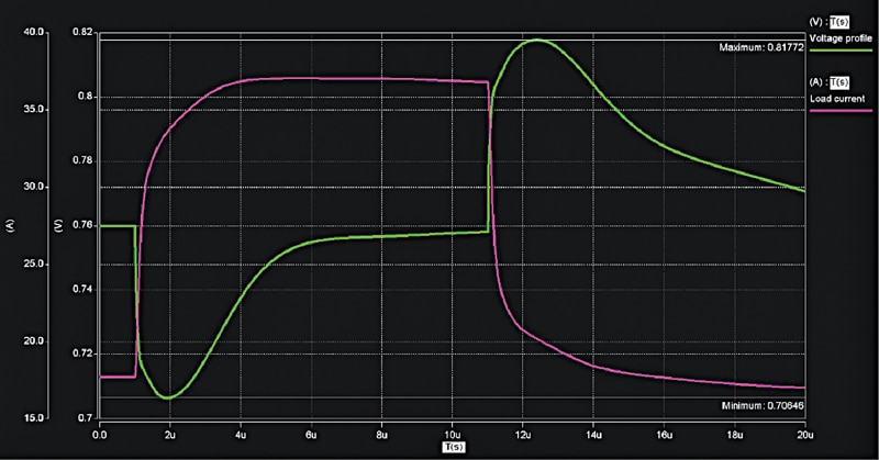
Fig. 7 displays an example of time domain voltage and current profiles for any PDN under analysis. A piece-wise linear current source connected at load terminal is used as a stimulus to excite the PDN. Here, the stimuli current rises from 17A to 37A in 1µs. In real work application, this type of load demand can be attributed to CPU operating in turbo mode of operation, that is, increasing its operating frequency to execute the workload.
With rise in current demand of the load, voltage at it input drops to a minimum level, governed by PDN impedance Z, and rises back to the steady-state level governed by its DC resistance. At about 10µs, the current demand falls suddenly, which could be attributed to end of workload execution and CPU reducing its frequency of operation. Due to sudden decrease in the load demand, voltage at the devices overshoots and hits a maximum value before settling back to the steady state.
The main aim of the entire exercise of power integrity analysis is to ensure minimum and maximum voltage levels at device input measured in simulation are within device operating range for reliable performance, and the simulation setup and results match closely with actual testing conditions and results.
Fig. 8 shows system power integrity analysis workflow. It starts with sanity check of system receivables followed by DC performance check. With DC criterion met, analysis flow moves to frequency domain analysis. In frequency domain analysis, impedance profile Z of the system is compared against ZTarget. If Z<ZTarget for system range of frequency operation, the analysis moves to the final stage of transient check or time domain analysis.
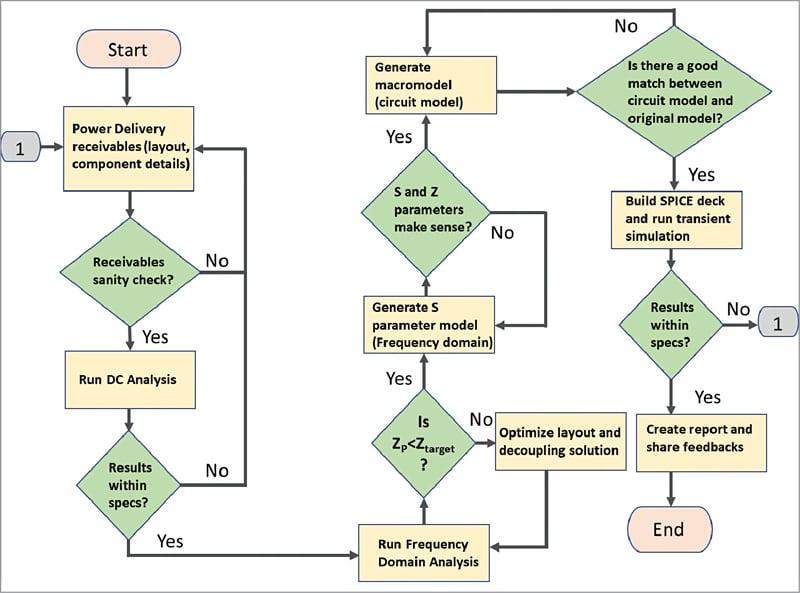
For time domain analysis, PDN circuit model is generated first followed by SPICE deck building. Once the computed voltage droop and overshoot meets the design specifications, the power integrity analysis is concluded with high confidence design readiness.
Conclusion
With modern-day complex multi-chipset systems, power delivery designs are becoming challenging and more critical than ever. A lot of root-cause failures in faulty systems can be somehow related to the power delivery. With power integrity analysis workflow, this process can be simplified. If it sounds too good to be true, let’s clarify that it does amount to considerable work and investment during the design phase of the product. However, it ensures smooth design validation, reliable product performance, and better customer experience, which at the end translates to better sales and profits, which are the ultimate goals for any organisation.
Ashish Sharma is from Intel Technology India Pvt Ltd, Data Center Power Solutions, Bengaluru and Jagan Kandi is from Intel Corporation, Data Center Power Solutions, Chandler, USA. They would like to acknowledge Datacentre Engineering Group, Intel Corporation for sharing vital information and Fig. 2 through Fig. 6 that helped formulating this article.