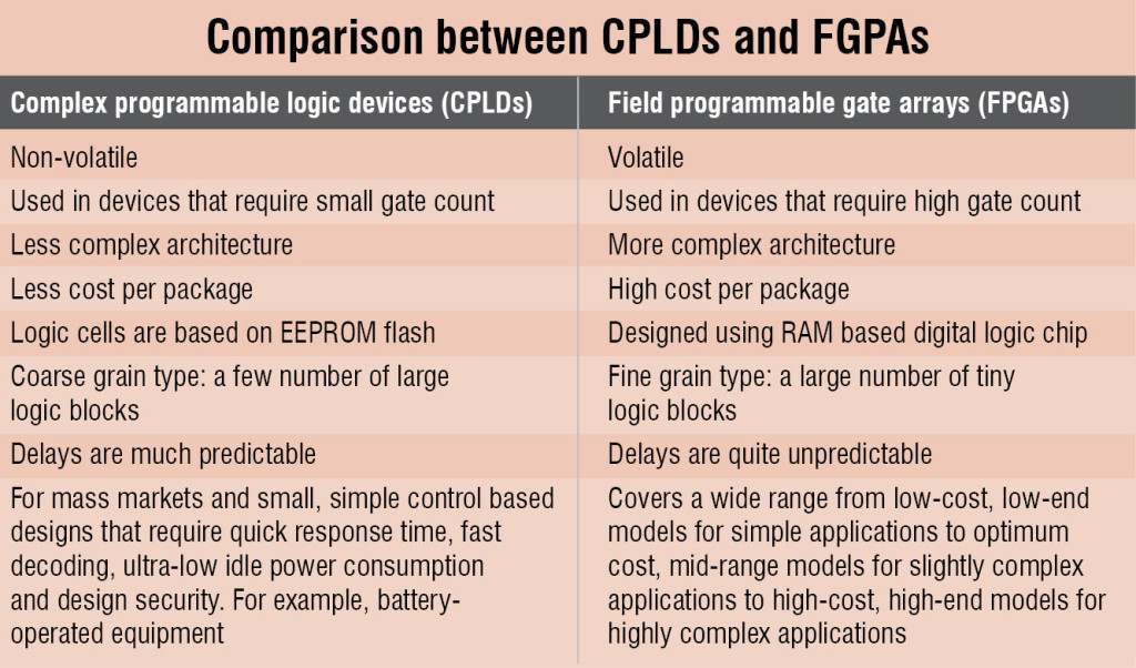
Programmable logic device is the name used to describe mainly two types of chips—complex programmable logic devices (CPLDs) and field programmable gate arrays (FPGAs).
“Programmable integrated circuits (ICs) were initially simple, logic based devices,” says Giles Peckham of Xilinx. But now the technology has advanced to a level where programmable ICs that we get these days are highly integrated and have a reduced footprint.

Hardware trends
As in most other fields of electronics, integration and size reduction are the two major trends that manufacturers are working on.
Integrating multiple features. “An exciting development in the field of programmable ICs was the release of flash based FPGA with built-in ADCs, DSP blocks, embedded internal memory and external memory,” observes Natarajan MM of Arrow Asia-Pacific. This product caters to the mass market and opens up new markets and new segments, like automotive, industrial, the Internet of Things (IoT) and consumer electronics. He adds, “More integration of hard system/IP blocks, like hard floating point DSP blocks, high-speed SERDES (serialisers/deserialisers), hard memory blocks, analogue-to-digital converters (ADCs) and 32-bit/64-bit ARM processors, is also seen.”
Integration of the processor into an FPGA takes it to the level of a programmable system on chip (SoC). This integration allows for faster system performance and greater flexibility, and allows for designers to differentiate their end-product by customising both hardware and software. It also reduces system cost and increases productivity for designers.
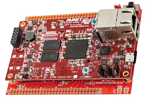
Powering SoMs. In an interaction with Dilin Anand of EFY (featured in this issue of EFY), Avnet’s Bryan Fletcher, technology director for global technical marketing, and Ramani Sundaresan, managing director for India, had mentioned the immense possibilities open to a design engineer when using system on modules (SoMs)/computer on modules (CoMs), powered by FPGAs. With sequential processing capabilities of SoMs and broad massive parallel programmable logic processing capabilities of FPGAs, a programmable SoM powered by an FPGA has both sequential processing and massive parallel processing combined together in a single system. Moreover, this is tightly coupled with thousands of connections internal to the chip. So you get the benefits of a processor and that of the programmable logic, using which you can accelerate the most critical tasks, and you have these very tightly coupled inside one package. Examples of such boards are ZedBoard, MicroZed and PicoZed from Avnet, Miami SoM from Topic Embedded Products and MitySOM from Critical Links.
An interesting example of an FPGA based SoM application is sensor fusion, where inputs from different types of sensors with different interfaces and different communication protocols are processed in real-time. The processor manages all incoming data sequentially and the programmable IC processes all these inputs in parallel in real-time.
Packaging. The density of an IC package is growing. Bigger designs are made possible with smaller chips. With increased density, the number of chips required reduces. This reduces interconnectivity, thereby decreasing the complexity of the entire design, increasing flexibility and offering better clock timings.
Seamless migration. One feature programmable IC firms offer is easy migration between different models of the same brand. This gives the user the possibility to upgrade from or replace an older, low-end version to the latest, mid-range or high-end version of FPGA.
Enabling tools
Major enhancements have been made in software tools for programmable devices. The software is now available with numerous built-in features that save a designer’s time in repeating the design process. Such advanced tools take care of so many factors that make the software much easier to use and increase the designers’ productivity by better reporting and increased performance, including common connectivity blocks to accelerate development cycle. Software flow for programmable devices is also becoming more flexible by allowing designers to adopt their own flow or architectures, like MATLAB/Simulink, ARM DS5, OpenCL and high-level synthesis (HLS).
The HLS of Xilinx Vivado design suite allows the user to write programs for ASICs and FPGAs in C and C++ languages, and easily convert these to hardware description languages (HDLs). So, even software engineers can now design with FPGAs. This is a big productivity boost for customers, as many people know C and C++ but not HDL, VHDL and Verilog. Software tools, like software-defined specification environment for networking (SDNet) and SDAccel by Xilinx, are software development environments for FPGAs and/or SoCs. These tools help in better hardware and software partitioning and improve design integrity.
The DesignInsight technology by Tabula, which consists of architecture, chip design and Stylus compiler software, allows real-time observation, debugging and validation of individual logic cells of PLD in real-time (up to 2GHz).
Application and industry specific
FPGAs are programmable for all industries. But there are several stringent certification procedures and requirements to approve a device for certain applications, like military, automotive and medical. Due to this reason major FPGA manufacturers are now introducing FPGAs specific to certain fields of applications. These are becoming more ASIC-like. For example, Altera Enpirion PowerSoCs and Cyclone V SoC FPGAs are automotive grade, Altera Arria 10 FPGAs and SoCs are fully-compliant with military standards, and Kintex Ultrascale is suited for data centres, video and medical imaging, broadcast systems and radars.
Data centre acceleration. Apart from working closely with CPUs and improving response time, throughput and efficiency, FPGAs these days also make programming and debugging easy by letting designers work in languages and architectures they are familiar with, such as MATLAB/Simulink, OpenCL, ARM DS-5 and HLS. This is a major advantage to data centre programmers.
Network enrichment. The IoT environment is varied and uncertain, mentions Steve Gabriel, corporate communications manager at Altera Corp. The fast, computationally efficient programmable chips are suitable for the IoT segment in terms of power efficiency, time sensitivity and security. These are effective for IoT hubs that have to support a large number of ultra-low-power network protocols, constantly evolving safety and security tasks, and a wide variety of application-dependent, real-time computing loads.
Real-time 3D medical imaging. Medical image processing and analysis are computationally-intensive tasks and require larger memories. The use of programmable chips, like high-powered CPUs and FPGAs, allow real-time, high-speed and accurate processing and analysis of photonic and electronic signals, with high image resolution. It is also comparatively lower priced, flexible, has a longer lifetime and allows continuous update of features and algorithms with the help of software toolsets, such as Altera video and image processing (VIP) suite. This can be used in positron emission tomography (PET), optical coherence tomography (OCT), computerised tomography (CT), X-ray imaging, ultrasound scanning, image guided therapy and so on.
For medical equipment manufacturers. A handheld hardware platform that lets you drag and drop sensor algorithms between the processor and FPGA fabric, and instantly observes resulting trade-offs in performance and power consumption, is being developed by Netherlands based Topic Embedded Products in collaboration with Xilinx. This would serve as a complete clinical reference design platform for medical equipment manufacturers.
In automotive industry. With autonomous driving becoming a reality in coming years, demand for technologically-advanced features, like automated braking, lane tracking, pedestrian detection, traffic sign recognition and parking assistance, have translated into a myriad list of challenges for system designers. With evolving safety, security and reliability standards for a vehicle, FPGAs offer a scalable, highly-reliable and power-friendly platform with reduced form factor and bill of material (BoM). A typical intelligent car has greater than 60 electronic control units (ECUs).

“Designing such a hard, real-time, low-latency gateway unit requires the right combination of hardware and software intellectual properties (IPs), driven by a system software capable of exploiting the best performance from underlying hardware,” says Bhaskar Das of Robert Bosch Engineering and Business Solutions. “The flexibility and scalability offered by FPGAs allow system designers to experiment, benchmark and quickly arrive at an optimal system design that rightly balances hardware and software needs,” he adds.
Which programmable chip is best suited for an application
Here are a few factors based on which the programmable IC for any application could be selected.
Logic requirement. Logic requirement of an application plays an important role in FPGA selection. If the application is simple and requires only about thousands of logic cells, CPLDs can be used. For low- and medium-complexity projects that require a hundred thousand logic cells or more, low-end and mid-range FPGAs are the options. High-end FPGAs with millions of logic cells are used for very complex applications.
System blocks/design requirement. From simple logic cells, programmable ICs have reached a level of high integration where several features and functions, like DSP blocks, PCIe blocks, processors, mixed signals and memory, are integrated into the chip. Altera’s Arria 10 FPGAs and SoCs have integrated ARM processors, Cypress PSoC integrates configurable analogue and digital peripheral functions, memory and microcontroller on a single chip, and Lattice iCE40 Ultra integrates emerging infra-red remote, barcode, touch, user identification and pedometer functions.
I/O. Input/output requirements, like voltage, SERDES interface standards and others, can be deciding factors while selecting a programmable chip. For example, Altera Arria 10 supports double data rate random access memory (DDR4 RAM) interface with high data rates. Similarly, Xilinx Ultrascale family has a hybrid memory cube (HMC) interface.
Price. The cost of CPLDs is less as compared to FPGAs. Many medium complex designs are more cost- effective at 28nm node of FPGAs. 16nm node is generally for high-end designs and costs more.
What the future holds
Adoption of 14nm FinFET technology has given the programmable industry a much needed boost in terms of high performance, lower cost and lower power, and has bridged the gap between FPGAs and ASICs even closer. Chip manufacturers are now moving towards 10nm technology. Natarajan believes that Intel’s partnership in the programmable space will lead to more breakthrough innovations and allow programmable devices to meet the ever-increasing demand of customers.
Gabriel states that the two emerging trends in the industry—data acceleration and network enrichment—are addressing the need for faster and predictable real-time performance, low-power Wi-Fi and Ethernet connections, and rapidly-evolving device security. “As the industry is struggling to make the IoT work, these two trends play directly into the strengths of, while creating great opportunities for, programmable logic,” adds Gabriel.