


There is always room for improvement in the world of technology. But it can only be improved and never perfected. System processors have seemingly come a long way, arguably even peaked. Let us if that is really the case or not.
If you look at the performance and the growth of general-purpose computers, you will see that they had a spectacular growth from the 1980s all the way to 2000. But thereafter it slowed down considerably to 12% a year, and currently the rate is down to 3% a year.

But there still seems to be a lot of room available where you can make computer architecture adapt to do domain-specific customisations. We submitted a proposal to the National Science Foundation US, back in 2008, which got us the funding to establish a centre for domain-specific computing.
The goal at the time was to look beyond parallelisation and focus on domain-specific customisation to bring significant power-performance efficiency. Recently we have released a paper which talks about the research that has been done in the past decade.
Successful examples of customisation
The best possible example of customisation is the Google Tensor Processing Unit (TPU). Its first version was released in 2017. It was subsequently upgraded from DDR3 to DDR5 where the bandwidth went up to 188 gigabytes per second. At the time it was 200 times faster than a general-purpose central processing unit (CPU) and 70 times more energy-efficient.
In the last five years both the CPUs and graphics processing units (GPUs) have improved significantly. The problem however is that not everyone can do such a design, because doing such designs requires millions of dollars. It can take 12 to 24 months on average to build a project like this.
Customisation for the masses using FPGAs
Everyone wants to do customisation today for which we can use field programmable gate arrays (FPGAs). They consist of a lot of configurable logic blocks or lookup tables which can be customised to implement logic functions. They also have a number of dedicated components, for example, memory/multipliers and I/O processors, which provide additional efficiency.
If you have generated bit streams then you can reprogram FPGAs in seconds and get new functionality. They are also very affordable. The only shortcoming that the FPGAs have is that they have lower density and clock rate compared to application specific integrated circuits (ASICs). Let us now take a look at a few examples.
Example 1. Scalable sorting. We designed a multiple FPGA based sorting entrance. Here is one that we have for a D1 level sorting:
Phase 1: Multiple merge trees work with multiple HBM channels concurrently.
Phase 2: Merge trees are reused from phase 1 with extra logic to build a wider tree.
As a result, we can sort four gigabytes of data in 0.25 seconds.
Example 2. This is a case from Microsoft. In this case they have an FPGA that is considered as a “bump-in-the-wire” before they connect to that data centre switch. This allows them to do a lot of on-the-fly computation. This was done by Microsoft to accelerate deep learning.
Why general-purpose processors are falling behind
General-purpose processors are powerful. You can implement any instructions you want. There is an instruction called the exclusion pipeline. If you just want to add an operation, then you will have to fetch the instruction and decode it to know which instruction it is.
Sometimes, the data may not be available if you want to rename one of the operands or both operands in order to avoid the name conflict, for which you will have to schedule in a renovation station. You can execute all the data in the arithmetic logic units (ALUs) once all the data is available.
If you are doing an out of order execution, then you will have to have a realtor buffer so that everyone before you is committed and you can write it back.
Power of customisation (domain-specific accelerators)
Following are some of the powers of customisation:
- Special data types and operations. Get things done in just one cycle what normally takes tens or hundreds of cycles.
- Massive parallelism. This increases the performance but not the efficiency.
- Optimised memory. It provides high bandwidth (consumes low energy) for specific data structures and operations.
- Reduced or armortised overhead. Provides 10,000 times efficiency gains for simple operations.
- Algorithm-architecture co-design can also be done.
Now, this raises the question, why everyone is not designing their own customised accelerators? The reason is that most people in the IT industry are software developers. There are only 66,000 persons who are considered computer power engineers, which makes the FPGAs (and ASICs) designing quite challenging.
What about high-level synthesis (HLS)?
HLS tools allow you to do a C based synthesis. HLS supports standard floating point operations and it consists of a lot of special optimisations. It fully supports IEEE-754 floating point data types and operations. It can efficiently handle bit-accurate fixed-point arithmetic. The quality of result matches or exceeds manual RTL for many designs.
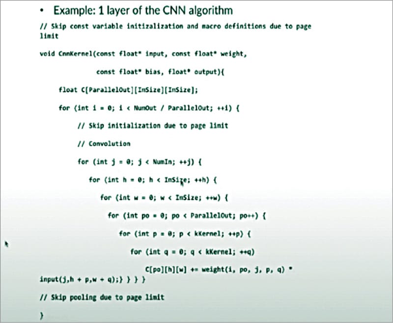
However, not all C programs lead to good performance. Let us take a very simple example like a convolutional neural network (CNN). Basically, for every output image you will have to do this convolution. It has to be done for every row and column. You just have to feed this code (see figure) into that high-level synthesis tool.
You do get a circuit, but it is 80 times slower than even a single-core central processing unit (CPU). You just have to take the parameters (const float* input, const float* weight, const float* bias, float* output) and map them into the device DRAM.
When you design your own accelerator, you have to get the cache from D1 every time, unless you have specified. If you don’t do any parallelisation, then all these loops will be executed sequentially. It is important to remember that in FPGA the clock frequency is typically five times slower.
What it takes to get a good HLS design? Since the speed is lower than a single-core CPU, students are not satisfied with the results, hence, they optimise it. They introduce on-chip buffers to cache the data, and they do fine-grain pipelining, fine-grain parallelisation, and coarse grain pipelining so that computation can be overlapped with communication. At the end, memory partition is done in order to maintain concurrency.
Making customised computing accessible to everyone
We want a software programmer to start with the language they are familiar with, for example, TensorFlow, SPARK, or any kind of basic language they can start with—at least C or C++. We compile it into some intermediate representation internally for which we have HeteroCL[FPGA’19]/MLIR.
MLIR is a community-wide effort that was originally started by Google and Intel. They are working to create automatic customised architectures, such as Systolic arrays and Stencil computation, and there is also a new type of architecture with product compostable parallel and pipeline (CPP).
If you have a certain pattern then we can generate this automatically for you. If not, we can use machine learning techniques to look for the best optimisation. As a programmer, you just have to write an efficient CPU code.
Our manual systolic array design experience has been decent so far. We started this effort back in 2014 without knowing what Google had been doing.
We independently designed a systematic way for matrix multiplication with the help of a very bright undergraduate student. It was a manually designed 1D systolic array with over 1700 lines of RTL code. We did get a running close to 200 GFLOPs on Xilinx VC709.
A closer look at computation management throws up the following:
Space-time mapping. Transforms the program to a systolic array with space-time mapping.
Array partitioning. It partitions the array into smaller sub-arrays to fit limited on-chip resources.
Latency hiding. Permutes parallel loops inside to hide computation latency.
SIMD vectorisation. Vectorises computation to amortise the PE overheads.
We have adopted the Merlin compiler, which was developed by Falcon Computing. It is similar to OpenMP for parallel computation, with which many of you are already familiar.
You can write programs like #pragma ACCEL parallel, which runs multiple loop iterations in parallel (instruction/task-level). Inside the compiler you can automate transformation. It allows you to perform on-chip memory banking/partitioning/delinearisation, external memory bursting/streaming/
coalescing.
| Overview of AutoSA compilation flow |
| Today, we have a completely automated tool. It extracts the polyhedral model from the source code and examines if the target program can be mapped to the systolic array. It constructs and optimises PE arrays (space-time mapping, array partitioning, latency hiding, vectorisation) and I/O network (I/O network analysis, double buffering, data-packing). It also generates target hardware code. |
Current goal: Zero pragma
We need to build things on top of what we already have. For example, if you want to do double Matrix vector multiplication, and you have some good hardware design tuition, then these pragmas are reasonable, and this is what we want to remove completely. (A pragma is a compiler directive that allows you to provide additional information to the compiler.)
We are going to do this using various machine learning algorithms. Along with this we are also going to use several deep learning models. This will be done in following steps:
Step 1: Create a database for training the model. We are going to take the C++ code and run it in the Merlin compiler. We will be getting a solution, which we will analyse. This will help us find the bottleneck, which will allow us to pipeline the rows. We essentially train a machine learning agent and we do it for a whole bunch of applications.
Step 2: Represent the program as a graph. We need to build the graph using the LLVM IR to capture lower-level instructions. We need to include both the program semantic and pragma flow in the graph (program semantic: control, data, and call flow). The graph is generated once per kernel and filled with different pragma values later on.
Step 3: Build a predictive model. From here we are going to create a graph of neural networks. We will first do the encoding here. Each node consists of a feature and you are going to compute a new feature iteratively based on your neighbours. This matrix can also be learned. It is similar to deep learning for images. Eventually, after adding them all together, we will get a graphing value that represents the program.
Other efforts to make FPGAs easier to program
- We can support legacy code (for example, with pointers and recursions): HeteroRefactor.
- We can support task level parallelism: TAPA.
- We can do performance debugging.
- We can do better integration for near-storage acceleration: Insider.
- We can improve the clock frequency for HLS design: AutoBridge.
This is a golden age for computer architecture, and we want to support every programmer who wants to participate and wants to build their own customised accelerators on field-programmable fabrics. And we hope that many people will be on board with us for the same.
This article is based on a tech talk session at VLSI 2022 by Jason Cong, Volgenau Chair for Engineering Excellence, and Director of VAST, UCLA. It has been transcribed and curated by Laveesh Kocher, a tech enthusiast at EFY with a knack for open source exploration and research.
Jason Cong, Volgenau Chair for Engineering Excellence, and Director of VAST, UCLA
