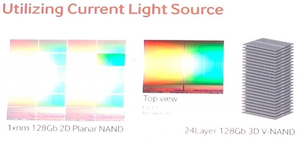
A wider bit line resulting from the vertical design solves this problem in the case of 3D V-NAND.
Photolithography and Patterning. Another problem that memory designers faced with smaller process nodes concerns photolithography. They had to find a light source that could pass through the smaller patterns created as a result of the newer manufacturing process. Patterning was used to overcome this problem and enhance density. The patterning process allows for geometries half as wide as what the scanner is capable of printing, but it has its limits within the 10 nm process range.

In 3D V-NAND, stacking the vertical layers in three-dimensions allows designers to increase capacity without being restricted by the limitations of patterning.
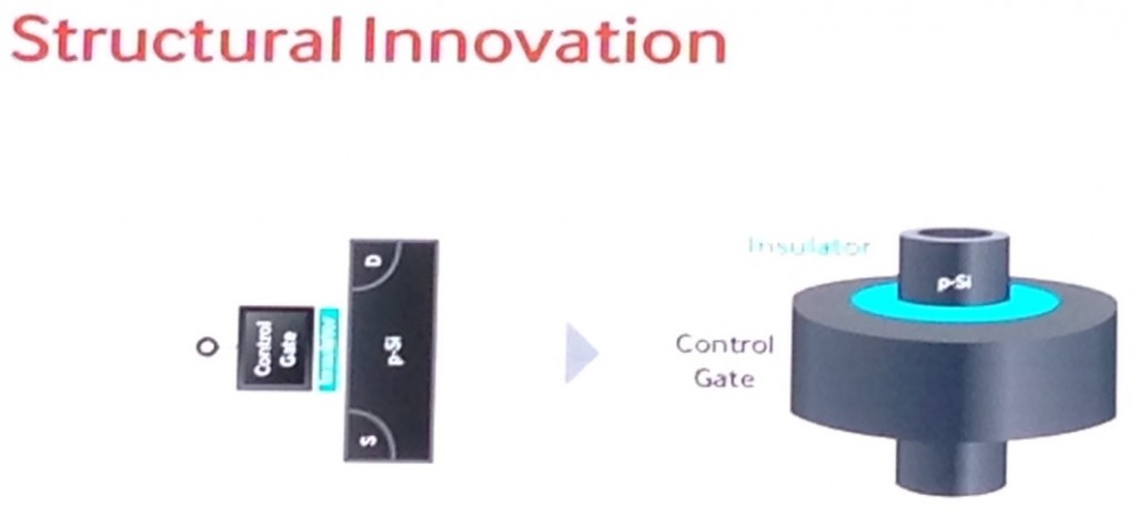
Construction Material. The basic construction material used in NAND memory has also changed in the transformation from 2D Planar NAND to 3D V-NAND technology. While the former used conductors, the 3D version uses insulators to enable the cells to hold their charges after writing data.

What does this mean for the user?
One of the biggest and most obvious benefits that the new technology offers users is the increase in capacity. With 3D V-NAND, it is possible for SSDs to store up to 1 TB of data on a single drive.
As cell-to-cell interference is now out of the picture, the programming algorithms implemented for storage can be far simpler than the current versions.
Finally, using an insulator rather than a conductor as the material increases the endurance, as insulators are less prone to wear and tear than conductors and it is claimed that this can result in an endurance that is 10 times higher.
Apart from being used in devices, this technology is bound to have a direct effect on data centres, where its benefits could push people to consider replacing HDDs with SSDs!
The author is a senior assistant editor at EFY.


