


DDR5, the fifth-gen DRAM, demands digital-analogue finesse in its MC and DDR PHY. Unique timings, coupled with emerging tech like 3D XPoint, MRAM, and ReRAM, mark a paradigm shift
Memory is typically used for storing the data or program code needed by a computer processor to function. To accomplish this task, Dynamic random access memory (DRAM) is employed. DRAM is a common type of random access memory (RAM) used in personal computers (PCs), workstations, and servers. Random access allows the PC processor to access any part of the memory directly rather than proceeding sequentially from a starting place.

How does DRAM work?
Memory is made of bits of data or program code arranged in a two-dimensional grid. DRAM stores bits of data in what’s called a storage or memory cell, consisting of a capacitor and a transistor. The storage cells are typically organised in a rectangular configuration. When a charge is sent through a column, the transistor in the column is activated. A DRAM storage cell is dynamic, meaning that it needs to be refreshed or given a new electronic charge every few milliseconds to compensate for charge leaks from the capacitor.
The memory cells work with other circuits that identify rows and columns, track the refresh process, instruct a cell whether or not to accept a charge, and read or restore data from a cell.
DRAM is one option of semiconductor memory that a system designer can use when building a computer. Typical sizes of DRAM are about 1 to 2GB in smartphones and tablets and 4 to 16GB in laptops.

Advantages of DRAM
- Very dense
- Low cost per bit
- Simple memory cell structure
Disadvantages of DRAM
- Complex manufacturing process
- Data requires refreshing
- More complex external circuitry is required (read and refresh periodically)
- Volatile memory
- Relatively slow operational speed
Manufacturing processes involved in DRAM
DRAM manufacturing processes are referred to as 1x-nm, 1y-nm, 1z-nm, 1alpha-nm, and 1-beta. A particular dielectric layer is provided to achieve the capacitance for each bit cell. 1beta DRAMs are low-powered and have double data rate 5X (LPDDR5X), capable of delivering data at a rate of 8.5Gbps. Multi-pattern lithography, in combination with leading-edge process technology and advanced material capabilities, is required for the manufacture of 1beta node DRAMs. The introduction of enhanced dynamic voltage and frequency scaling extensions core (eDVFSC) techniques is used to improve power-saving controls of DRAMs.
1-gamma node DRAMs are coming
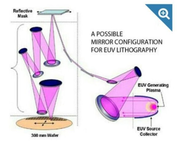
This advanced DRAM is expected to unlock exponential growth and opportunities for an increase in the digital economy. It is a major step to secure the semiconductor supply chain. Currently, Micron is a pioneer in DRAM manufacturing. Recently, it installed extreme ultraviolet (EUV) lithography production equipment at its A3 wafer fabrication unit in Taiwan.
In May 2023, Micron announced that it will be introducing this sophisticated pattern technology (EUV) to manufacture its next-generation DRAM, 1-gamma node. This technology is expected to provide the smallest cell size for DRAM. The downside of EUV lithography is that it needs multi-patterning, allowing 193nm lithography to considerably reduce the size of DRAM. Micron is combining new materials, tools, and novel techniques to improve its multi-patterned alignment.
| Table 1 SRAM Vs DRAM | ||
| Parameter | SRAM | DRAM |
| Read/write speed | Faster | Slower than SRAM |
| Power consumption | More | Less |
| Internal structure | Complex | Simpler than SRAM |
| Density | Less dense | Highly dense |
| Used in | Cache memory | Main memory |
| Storage per bit | Can store more bits per chip | Cannot store many bits per chip |
| Storage component | Transistor | Capacitor |
| Price | Expensive | Economical than SRAM |
Challenges Faced by DRAM Industry
One-die Error Correction Code (ECC) is a special feature in the DRAM industry that corrects bit errors in DRAM chips, increasing reliability and defect rates. ECC requires additional memory storage where ECC codes are stored at the time of memory write to DRAM. Hamming codes are used in such ECC schemes to provide single-bit and double-bit error detection per burst. Latest DRAMs like LPDDR5 and DDR5 support one-die ECC.
Row hammer
The same or adjacent rows are activated again and again, resulting in a loss or change of data contents in the rows that are not addressed. The latest versions of DRAM LPDDR5/DDR5 support refresh management (including DRFM and ARFM) to compensate for this challenge
Device temperature
Users need to check with the DRAM vendor on the temperature range where DRAM should operate. Data integrity is lost at a level greater than a certain temperature.
Loss of power
DRAM may lose its contents due to a loss of power. So, a backup non-volatile memory is required where DRAM contents need to be copied before the power is lost. When power is regained, stored contents in non-volatile memory are written back to DRAM.
Specifications of DDR5 and Lpddr5 as set by the Joint Electron Device Engineering Council (JEDEC), which is an industry standards body and governs specifications of DRAMs, are given in Table 2.
| Table 2 Specification of DDR5 and Lpddr5 | ||
| Factor | DDR5 | Lpddr5 |
| Maximum die density | 64Gbit | 32Gbit |
| Max. data rate | 6.4Gbps | 6.4Gbps |
| Max. UDIMM size (DSDR) | 128GB | N/A |
| Channels | 2 | 1 |
| Channel width | 64 bits (2×32) | 16 bits |
| Memory banks | 4 | 16 |
| Bank groups | 08/04/23 | 4 |
| Burst length | BL 16×2 | BL 16 |
| Prefetch | 16n | 16n |
| Voltage( Vdd) | 1.1V | 1.05V |
| Vddq | 1V | 0.5V |
DDR5 MC and PHY
DDR5 is described as the fifth-generation Double Data Rate Synchronous DRAM designed for next-generation computing. DDR5 Memory Controller (MC) and DDR PHY are two major components for efficient DRAM performance. DDR5 MC needs digital design experts while DDR5 PHY needs both digital and analogue expertise. For each application, DDR5 has a large number of timing parameters and configuration registers. Each vendor has to own its own unique timing parameter and configuration register values. DDR5 PHY Interface (DFI) is an interface protocol that defines timing, signals, and programmable parameters required to transfer data to and from DRAM to MC. In many situations, MC and PHY are designed separately and often by different companies.
Next generation DRAMs
Current DRAMs increase latency and power consumption, known as the ‘memory wall.’ Next-generation DRAMs have come up with new features to overcome these challenges. Introduced by Intel in 2015, 3D XPoint is described as the next generation DRAM. 3D XPoint is based on a technology called Phase-Change Memory (PCM) and is used in SSDs and DIMMs. PCM stores information in the amorphous and crystalline phases.
Meanwhile, the industry is also developing other new memory types, such as Magnetoresistive RAM (MRAM) and Resistive RAM (ReRAM). Like 3D XPoint, MRAM and ReRAM can be made and sold as standalone devices.
3D XPoint is not sold as an embedded memory. In contrast, MRAM and ReRAM can also serve in the embedded memory markets. For MRAM, the industry is developing a next-generation technology called Spin-Transfer Torque MRAM (STT-MRAM). STT-MRAM uses the magnetism of electron spin to provide non-volatile properties in chips, combining the speed of SRAM and the non-volatility of flash with unlimited endurance.
In traditional memory, data is stored as an electric charge. In contrast, MRAM uses a magnetic tunnel junction (MTJ) memory cell for the storage element. Ferroelectric RAM (FRAM) is another technology to watch. Using a ferroelectric capacitor to store data, FRAM is a non-volatile memory with large storage capacity. Nantero, a private company, has more than 170 nanotube patents to replace DRAMs. It is possible to have hundreds and thousands of such nanotubes in every memory cell to form a network of resistive elements to form non-volatile random access memory (NVRAM). Undoubtedly, next-generation DRAMs are providing plenty of opportunities for OEMs.
Our past, present, and future memory requirements in the e-world are much more than we expect. In the web world, information can be kept alive by memory. DRAM gives another view of e-memory, providing another understanding of the ‘data storage mechanism.’
The author, Vinayak Ramachandra Adkoli, is BE in industrial production and has served as a lecturer in three different polytechnics for ten years. He is also a freelance writer and cartoonist
