


Key to success of any product lies in its producibility, quality and reliability. Quality and reliability cannot be achieved by just arriving at a schematic to perform a required function and specifying component values. Many more steps are required to make a reliable product. Here we describe the design flow required to achieve a quality and reliable product, followed by other requirements.
Design methodology
Determine. Determine the product requirements such as:
1. Functions that the product has to perform. These functions are called requirements.

2. Operating conditions under which the product will perform its functions. These include temperature range, vibrational stresses and electromagnetic compatibility requirements. The operating condition is called lifecycle environment.
3. Conditions under which the product is to be stored and transported.
4. Power requirements (alternating current or direct current, voltage value, etc).
5. Electrical interface requirements (interfacing signals (analogue/digital), voltage range for analogue signals, serial input/output or parallel interface standard for digital signals).
6. Mechanical interface requirements (size, shape, material and finish).
7. Regulatory requirements, say, electromagnetic emissions.
Define. Define how best the unit should perform its function in terms of technical performance specifications—power output for a radio transmitter, sensitivity for a radio receiver and non-linearity for a measuring instrument.
Explore design concepts. Explore and evaluate alternative design concepts to meet the requirements determined.
Component selection. Select proven, standard and replaceable components from reputed manufacturers. If components with new technologies or sources are used, evaluate their performance for required functionality under required operational stresses (electrical, mechanical, thermal, etc).
Components should also be able to withstand stresses from handling, storage and assembly. Easy assembly should be possible. Care should be taken so that selected components do not become obsolete very soon. Design should use replaceable modules so that the unit can be repaired and maintained easily.
Performance analysis with electronic design automation (EDA) tools. Simulate the designed schematics with EDA tools. Initially use nominal values for all components in simulation. Confirm that the design is giving required outputs with required inputs. Correct any non-conformance by modifying the design and simulating again.
Tolerance analysis. Nominal component values are specified in the designs. It is, however, practically impossible to manufacture all the components exactly with required values. Hence allowable tolerances (upper and lower limits) are to be specified for the component values so that even when actual component values vary within designated tolerance limits, the design performs as required.
Simulate the design with component values set to extreme limits within the specified tolerance. Confirm that the design still performs well. Correct any non-conformance by modifying the design and simulating again.
Monte Carlo analysis. During production, all components in a particular unit will not be at their extreme tolerance limit values. In fact, actual values will vary from unit to unit randomly within the tolerance limit. This random variation can be modeled by Monte Carlo analysis.
Monte Carlo analysis simulates a hundred or thousand runs of the same schematic. It varies component values randomly within the set tolerance limits as per set distribution from schematic to schematic. The results can be analysed to determine the percentage of circuits that meet specification limits.
The results help determine whether the selected tolerance for components is adequate or not and whether it can be widened for some components. Wider-tolerance components cost lesser than narrow-tolerance components.
Margin (de-rating) analysis. A designed unit is required to function during its operational lifetime under expected operational stresses. The capability to withstand stresses (temperature, vibration, etc) varies from component to component. Component values and capabilities also vary/degrade with storage and time because of chemical and physical phenomena.
To accommodate these variations, units are to be designed to withstand more stress than required during operation. For example, if a unit is required to operate at 50°C, components that can withstand 70°C should be selected. Similarly, if a resistor consumes 0.25 watt during operation, a 0.5-watt resistor should be selected. This method of using components at less capability during operation is called de-rating. This is one way to design a reliable product.
One should also ascertain by simulation that the design performs satisfactorily at higher thermal (temperature) and dynamic (vibration) stresses than required during operation. This can be achieved by performing thermal and packaging analysis using EDA tools. This analysis is also called Margin analysis, as it ascertains that the design has margin compared to required operational stresses.
Printed circuit board layout and analysis. PCB layout pattern and design play an important role in the reliable performance of an electronic system. This is particularly true at high frequencies, where PCB tracks behave like transmission lines. This condition happens if signal transmission delay along the length of the PCB track is comparable with the rise and fall times of pulses. Pulses at the receiver will be distorted with ringing and not received by the receiver correctly. Pre-layout and post-layout signal integrity (SI) analysis using EDA tools needs to be done to examine this problem. Terminating resistors, if required, need to be added at appropriate places.
Care should be taken so that the loop area enclosed by signal current’s send and return paths is minimised. Larger loop area results in electromagnetic interference (EMI) to nearby circuits through mutual inductive coupling. It also makes the circuit under operation susceptible to EMI from nearby circuits.
Signal return current path is normally the circuit’s signal reference ground. This ground is shared by many signals. Ideally, ground should have zero impedance at all frequencies. Practically, ground tracks will have non-zero impedance (inductive), especially at higher frequencies. This results in non-zero voltage drop across ground, causing the transmitted signal to be received erroneously by the receiver. Care should be taken to ensure near-zero-impedance ground at direct currents to frequencies of interest. To achieve this, a large ground area should be used. If necessary, use a multilayer PCB with separate planes for ground and power supply.
Keep the following things in mind:
1. Use separate grounds for sensitive analogue circuits and noisy digital circuits.
2. Physically separate sensitive analogue circuits from noisy digital circuits.
3. The rise and fall times of pulses should not be less than required. Pulses with short rise and fall times will have a high frequency content and increased electromagnetic emissions.
4. Use power supply decoupling capacitors—one for every four to five digital integrated circuits (ICs). These are required to counter inductive voltage drop developed by switching currents in digital ICs.
5. Select the track width for signal and power tracks such that these can sink the required current.
6. Provide appropriate spacing between signal tracks to avoid cross-talk.
7. Select pads suitable to component dimensions.
8. Allow adequate clearances between tracks and through-hole component pads so that components can be easily soldered.
9. Use heat-sinks for high-power-consuming components like power amplifiers and power supplies.
10. Perform thermal analysis with EDA tools to find out hotspots on PCBs.
11. Only general guidelines are provided here. Study PCB layout literature for more details.
Packaging
Any electronic product normally has a number of PCBs connected by a motherboard. All the PCBs are placed in a metallic enclosure. The enclosure has connectors fixed to it for external communication of signals. Wiring harness runs from connectors on the chassis to the PCBs/motherboard.
Unit packaging is to be designed carefully such that the unit can withstand thermal, mechanical, electromagnetic and electrostatic discharge (ESD) stresses.
Thermal stress. Performance of many electronic components and systems degrades with temperature. This happens more when subjected to high temperatures for a long duration. Electronic components can also get mechanically damaged when temperature changes fast from high to low and vice versa.
The most common method of thermal control is use of heat-sinks. By employing a heat-sink, a low thermal resistance path is provided from the component to the air. Heat conducts from the component to the heat sink. Heat sink is cooled by convection, with air serving as the thermal reservoir.
Other techniques are:
1. In a forced-air-cooled package, spread the heat-dissipating parts uniformly along the cold wall.
2. Do not place thermally sensitive or highly dissipating parts close to each other.
3. Do not place thermally sensitive parts next to hotspots.
4. In free-convection-cooled equipment, do not place parts directly above highly dissipating parts; stagger them horizontally.
5. For contact interfaces, use as much contact area as possible.
Mechanical stress. Excessive mechanical stresses, such as vibration and shock, generated during operation of electronic sub-systems (for example, launch of missile systems) can cause chafed wiring, loose fasteners or components, intermittent electrical contacts, deformed seals, failed components, and cracked and/or broken structures.
Protection against mechanical stresses is generally achieved by suitable packaging, mounting and structural techniques. Two approaches used are mechanically isolating the equipment and building the equipment to required strength.
Packaging analysis using CAD tools is done to determine natural frequencies and mechanical stresses within components, produced by shock and vibrations. If stresses exceed safe levels, corrective measures such as stiffening and incorporation of further support members are required. An isolation system can be used at the source of vibration in addition to isolating the protected component. Damping devices can be used to reduce peak oscillations.
Humidity. Many electronic systems need to be stored and operated in coastal areas, which are highly humid. Humidity can cause corrosion, loss of mechanical strength, change of electrical properties and increased conductivity of insulators, thus degrading the performance of electronic systems.
Protection against moisture can be provided by applying protective coating, using hermetically sealed components and encapsulating materials with moisture-resistant waxes.
Electromagnetic interference (EMI). Electronic systems’ operation could be affected by electromagnetic interference caused by electromagnetic wave radiations. Sources of electromagnetic wave radiation include communication transmitters, radio broadcasting transmitters or radiation from circuits operating within a unit itself. Examples of EMI problems include noise created on a television set when a nearby grinder is operating, intermittent resetting of computers and noise heard in a radio set when a fluorescent lamp is switched on.
EMI problem also occurs when an electronic unit shares its source of power with other electronic units. This situation is called conducted susceptibility.
Effects of EMI can be minimised by:
1. Providing a metallic enclosure as equipment casing that isolates the circuits within from electromagnetic radiation
2. Using shielded cables
3. Using EMI gaskets to cover discontinuities in metallic enclosure at the places of connectors and cable entry points
4. Using EMI filters
Electrostatic discharge. When certain types of material come into contact and separate, electrons pass back and forth between them. One material gets positively charged and the other negatively charged, for example, when walking on a carpet or rubbing a plastic comb against dry hair. This phenomenon is called electrostatic discharge (ESD). The amount of charge and voltage developed depends on the materials, area of contact, speed of separation and relative humidity. The voltage developed could be as high as 20,000V.
Static voltage is generated in work areas by people during their normal movement. This voltage can cause malfunction of parts, assemblies and equipment or even damage them. Certain devices and technologies are more sensitive to ESD than others. Components that include field-effect transistors (FETs) such as complementary metal-oxide semiconductor (CMOS), high-frequency parts produced by Schottky barrier process and micro-circuits that utilise small active junctions are sensitive to ESD.
Failures caused by ESD could be intermittent, catastrophic or latent. In case of latent defect, the damaged device remains operational and fails some time later in its use.
General protection techniques to be followed to provide immunity against ESD are:
1. Select components that have inbuilt protection against ESD, or build protection in circuit design by using diodes, silicon-controlled rectifiers, metal-oxide varistors, etc.
2. Enclose the circuit in a metallic box and establish wire connection from the box to ground. Any static discharge will transfer from the box through the wire connection to ground. If a plastic enclosure is used, coat its interior with a conductive paint.
3. During production and assembly, components and sub-assemblies should be handled such that these are not exposed to ESD. This can be achieved by doing assembly in an ESD-controlled work area using ESD work benches with ESD straps and seats. These ensure that the operator or user is grounded.
4. Personnel doing assembly should wear ESD clothing to minimise ESD generation.
5. All components and assemblies should be stored in an ESD-controlled area.
6. All components and assemblies should be handled and transported in conductive or ESD-protective bags.
Others. Manufacturability, testability and maintainability aspects should also be considered during PCB, module and package design. Specialists in all fields should be involved from initial stages of design, in addition to core functional designers. This is called concurrent engineering. Get the design reviewed by experts in relevant fields with respect to all the given aspects.
Documentation
Documents need to be prepared that give information on materials and components to be used, as well as electrical and mechanical drawings. Documents are also required for any special instructions for components assembly, cable harness and integration, assembly sequence, acceptance procedures for individual components, materials, assemblies/sub-modules and total unit.
Prototype and qualification testing
Build a prototype and perform testing as per the documented procedure. Initially, prove functional performance under ambient conditions. Later, prove performance under higher stresses than required during normal operation—a process called qualification testing.
Qualification testing establishes design margins above required operating stresses for a unit. A design having a higher margin will help reduce rejections in production and reliability for a longer duration in the field. Analyse any failure to meet any requirement during this phase. Modify the design to meet the requirement. Modification could be required either in the circuit or packaging.
Critical design review
Get the design reviewed again by experts in relevant fields with respect to prototype qualification test results. Relevant modifications need to be incorporated in design documents.
Pilot production and acceptance testing
Now go for production of ten to fifteen units with qualification-test-cleared design. Component values are spread randomly among the units within tolerance limits. Complete performance testing as per the documented procedure at application stresses. This process is called acceptance testing.
With all the design steps given earlier followed, it is much less likely that any design problem will occur. Manufacturing problems are, however, likely to surface. Identify performance problems at this stage as manufacturing or design. Manufacturing problems can be solved by repair or rework. If any design problem surfaces, modify the design and confirm solution. Modify design documents accordingly. Major design modification might require qualification testing again.

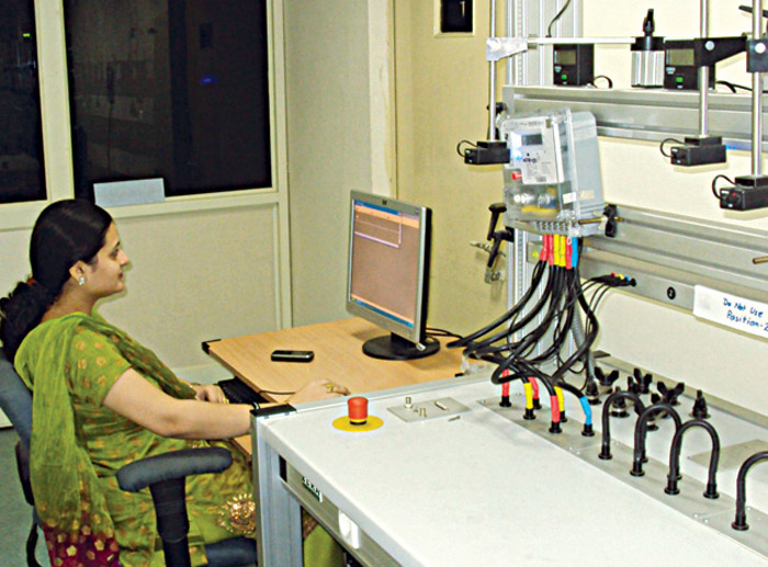
Production and quality control
The required level of quality and reliability is built into the product during design stage. It can be maintained in production only if correct materials and components are used, and correct assembly and manufacturing procedures followed as per design documents and drawings.
It is the responsibility of the quality control department to ensure that the design is translated correctly into a product during production by using right materials, components, assembly and manufacturing procedures as per design documents and drawings.
Failure reporting and corrective action
Any failure or non-conformance occuring during production quality control and testing is to be analysed by a failure analysis board to find out the root cause.
The cause needs to be traced to the manufacturing/assembly process or design. Required improvements are recommended and implemented to avoid recurrence of such failures.
Accelerated stress screening
A product is likely to fail in its initial stages of operation after it is delivered to the customer. This can happen if some manufacturing defects escaped industry quality control and testing procedures, or the unit was not subjected to testing under required operational stresses. These defects remain hidden in the product delivered to customers. Hidden defects precipitate under unit operational stresses at customer site for some time and lead to failure.
This situation can be avoided by testing the product at stresses higher than operational requirement but within design limits during manufacturing. Higher stresses will precipitate hidden defects in a shorter time than required under normal operational stresses at customer site.
Failed units can be reworked to remove manufacturing defects and delivered to the customer. This reduces the chance of the unit failing at the customer’s site in early stages of operation. This method of testing is called accelerated stress screening.
Reliability aspects
It is possible to estimate and predict the reliability of a design based on quality grades of components used and operational stresses. It is also possible to demonstrate reliability achieved by building certain number of units with the same design and using statistical methods. Reliability can also be estimated from field failure data.
The author is scientist-‘F’ and deputy director in Reliability and Quality Assurance Directorate of Research Centre Imarat, Defence Research & Development Organisation, Hyderabad