Field-programmable gate array (FPGA) is a device that has numerous gate (switch) arrays and can be programmed on-board through dedicated Joint Test Action Group (JTAG) or on-board devices or using remote system through Peripheral Component Interconnect Express (PCIe), Ethernet, etc. FPGAs are based on static random-access memory (SRAM). The contents of the memory of an FPGA erase once the power is turned off. Usually, FPGAs can be programmed several thousands of times without the device getting faulty.
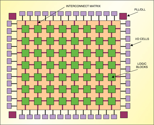
Fig. 1 shows the architecture of an FPGA. It includes logic blocks, input/output (I/O) cells, phase-locked loops/delay-locked loops (PLLs/DLLs), block RAM and interconnecting matrix. Nowadays, FPGAs are also coming up with several hard intellectual property (IP) blocks of PCIe, Ethernet, Rocket I/O, PHYs for DDR3 interfaces and processor cores (for example, PowerPC in Xilinx Virtex-5 FPGA and ARM cores in both Xilinx and Altera series FPGAs).
To level up with the new technology, both Xilinx and Altera have come up with new series of FPGAs (Virtex 7 from Xilinx and Stratix-V from Altera), which are manufactured with TSMC’s 28nm silicon technology. These FPGAs focus on a high speed with low power consumption using various parameters and bringing down the FPGA core voltage to as low as 0.9V. Along with the new FPGAs, Xilinx and Altera are also focused on improving their synthesis tools to meet the routing constraints and to analyse the timing and power consumption of the FPGA.

Fig. 1: FPGA architecture (generic)
As the aim here is to learn the basic technique of FPGA design to work with both the tools and devices, let’s get back to the design flowthrough the steps.
Step 1: Requirement analysis and SRS preparation
Before starting work on the design, all requirements should be documented as system requirement specificatio (SRS) by designers and approved by various levels in the organisation, and most importantly, the client. During this phase, FPGA designers, along with the hardware team, should identify suitable FPGAs for the project. This is very important because designers need to know parameters such as the I/O voltage levels, operating frequency and external peripheral interfaces.
It is also important to determine which IP cores are available with the tools or FPGA family used for the project. Some IP cores are free, while others are licensed and paid for. This cost should be reviewed several times by the team before releasing it to the client and listed separately for approval from the client or management.
The SRS should contain the following (the list pertains to the FPGA only):
1. Aim of the project
2. Functionalities to be handled by the design, followed by a short description
3. A concept-level block diagram depicting the major internal peripherals/IPs of the FPGA
4. FPGA vendor, family, speed grade, package, core voltage, supported I/O levels, commercial/industrial type
5. List of blocks that will be used as IPs. Mention clearly what’s available for free with the vendor-provided IPs, hard IPs available within the FPGA and paid licensed IPs to be used
6. Type of processor interfaces used (soft processor or external processor interfaces)
7. Type of memory interfaces used
8. A section about the timing diagram of the major peripheral interfaces such as the processor interface and flash interfac
9. Type of FPGA configurationsto be used
10. Reset and clock interface planned
11. A brief summary of the estimated resources required for implementation of the logic and I/O pins to be used
12. HDL (VHDL, Verilog, ‘C’ or mixed) used for RTL coding, tools and version to be used for synthesis, implementation and simulation

Spartan-6 USB-FPGA module 1.11b
To calculate the approximate resources required, go through the IP datasheets for the resources used for each IP, and also calculate the resources used by custom RTL. There is no rule of thumb for calculating resources at this level. These can be calculated approximately based on experience, reviews or analysis. The most important thing is to get the resource requirement reviewed by the hardware team, software team and a third party several times before submitting it to the client.
Step 2: Detailed design document preparation
Once the SRS is approved by the client, the next phase is to make the detailed design document.
This document should consist of:
1. Brief introduction to the project
2. FPGA part details with proper specification
3. Detailed block diagram depicting the internal modules of the FPGA design
4. Top-level module block diagram showing input and output ports with their active levels and voltage levels which are connected to the external peripherals, connectors and debug points
5. Hierarchical tree of the modules
6. Each module should have:
(i) Detailed explanation of the functionality
(ii) Register information
(iii) List of input and output ports with source and destination module name, and active level of the signal
(iv) A block diagram/digital circuit diagram of finite-statemachines indicating how the RTL will be implemented
(v) Clock frequency to be used, if a synchronous module is used
(vi) Reset logic implementation
(vii) File name which will be implemented
(viii) Approximate FPGA resource utilisation
(ix) Testbench for testing each module independently
7. Input system clock frequency and reset level


