FPGAs are reprogrammable hardware devices that offer high speed, flexibility, and real-time performance, making them ideal for parallel and time-critical applications. Compared to CPLDs, FPGAs are more flexible and complex, while CPLDs offer simpler, more predictable architectures. Microcontrollers, on the other hand, are software-driven computing systems suited for sequential control tasks but cannot match the parallel processing and deterministic behavior of FPGAs. This article explains FPGA architecture, types, advantages, limitations, and helps you choose between FPGA, CPLD, and microcontrollers based on application needs.
Table of Contents
Ever since Xilinx introduced to the word ‘field-programmable gate arrays,’ popularly known as FPGAs, these have been extensively used for various applications. The name ‘field-programmable’ originates from the fact that an FPGA can be configured by a customer or a designer after manufacturing rather than during fabrication.
In essence, an FPGA is a two-dimensional array of generic logic cells and programmable switches that is configured using hardware description language (HDL), very high-speed integrated circuit hardware description language (VHDL) and VERILOG to name a few. FPGAs can be used to implement any logical function that an application-specific integrated circuit (ASIC) could perform. Some of the reasons for its popularity in modern electronics are its ability to update the functionality after shipping, partial re-configuration of a portion of the design and low engineering costs relative to ASIC design.
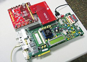
FPGAs contain programmable logic components called logic blocks, and a hierarchy of reconfigurable interconnects. A logic cell can be configured to perform a simple function, and a programmable switch can be customised to provide interconnections among the logic cells. A custom design can be implemented by specifying the function of each logic cell and selectively setting the connection of each programmable switch. Once the design and synthesis is complete, you can use a simple adaptor cable to download the desired logic cell and switch configuration to the FPGA device and obtain the custom circuit. In most FPGAs, the logic blocks also include memory elements, which may be simple flip-flops or more complete blocks of memory.
In addition to digital functions, some FPGAs have analogue features. The most common analogue feature is programmable slew rate and drive strength on each output pin, allowing the engineer to set slower rates on lightly loaded pins that would otherwise ring unacceptably, and to set stronger, faster rates on heavily loaded pins on high-speed channels that would otherwise run too slow.
Another relatively common analogue feature is differential comparators on input pins designed to be connected to differential signalling channels. A few mixed-signal FPGAs have integrated peripheral analogue-to-digital converters (ADCs) and digital-to-analogue converters (DACs) with analogue signal conditioning blocks allowing them to operate as a system-on-a-chip. Such devices blur the line between an FPGA, which carries digital 1’s and 0’s on its internal programmable interconnect fabric, and field-programmable analogue array (FPAA), which carries analogue values on its internal programmable interconnect fabric.
Types of FPGA
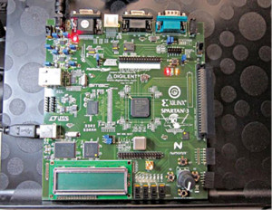
Major categories of FPGAs include SRAM-based FPGAs, Flash-based FPGAs and antifuse-based FPGAs. SRAM-based FPGAs store logic cells configuration data in the static memory (organised as an array of latches). Since SRAM is volatile and can’t keep data without power source, such FPGAs must be programmed or configured upon start.
There are two basic modes of programming: master mode and slave mode. In master mode, the FPGA reads configuration data from an external source, such as an external Flash memory chip. In slave mode, the FPGA is configured by an external master device, such as a processor. This can be usually done via a dedicated configuration interface or via a boundary-scan (JTAG) interface. SRAM-based FPGAs include most chips of Xilinx Virtex and Spartan families and Altera Stratix and Cyclone.
SRAM-based FPGA with an internal flash memory
This type of FPGA is similar to the conventional SRAM-based devices, except that it contains internal flash memory blocks, thus eliminating the need to have an external non-volatile memory. One example of such an FPGA is the Xilinx Spartan-3AN family (Fig. 1). Each model of Spartan-3AN has an on-chip flash memory module with an SPI interface capable of storing two or more configuration bit streams, which can be chosen during start-up. Internal non-volatile memory can also be useful to prevent unauthorised bitstream copying.
Flash-based FPGAs
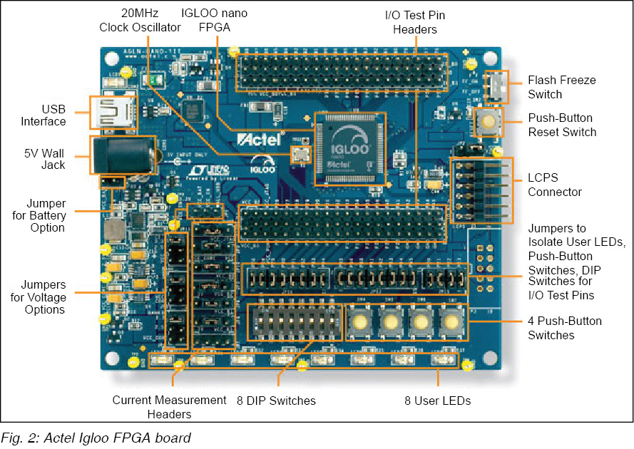
The true flash-based FPGAs shouldn’t be confused with SRAM-based FPGAs with internal flash memory. The SRAM-based FPGAs with internal flash memory use flash only during start-up to load data to the SRAM configuration cells. On the contrary, true flash-based FPGAs use flash as a primary resource for configuration storage, and don’t require SRAM. This technology has the advantage of being less power-consuming. Flash-based FPGAs are also more tolerant to radiation effects. Flash-based FPGA families such as Igloo (Fig. 2) and ProASIC3 are manufactured by Actel. As in the previous case, using flash-based FPGAs can be a solution to prevent unauthorised bitstream copying.
Antifuse-based FPGAs
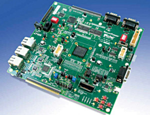
Antifuse-based FPGAs are different in that they can be programmed only once. The antifuse is a device that doesn’t conduct current initially, but can be ‘burned’ to conduct. Antifuse-based FPGAs can’t be then reprogrammed since there is no way to return a burned antifuse into the initial state. Antifuse-based device families include Accelerator (Fig. 3) produced by Actel.
Architecture
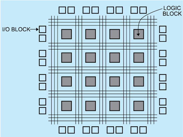
An FPGA consists of an array of uncommitted configurable logic blocks, programmable interconnects and input/output (I/O) blocks. Fig. 4 shows the basic architecture of an FPGA.
FPGA architecture is dominated by programmable interconnects, and the configurable logic blocks are relatively simpler. Logic blocks within an FPGA can be small, called fine-grained architecture, or larger, called coarse-grained architecture.
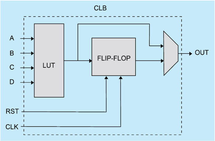
Fig. 5 shows the schematic of a typical logic block of an FPGA. It consists of a four-input look-up table (LUT) whose output feeds a clocked flip-flop. The output can either be a registered or an unregistered LUT output. Selection of the output takes place in the multiplexer.
An LUT is nothing but a small one-bit-wide memory array with its address lines representing the inputs to the logic block and a one-bit output acting as the LUT output. An LUT with ‘n’ inputs can realise any logic function of ‘n’ inputs by programming the truth table of the desired logic function directly into the memory.
Logic blocks can have more than one LUT and flip-flops also to give them the capability to realise more complex logic functions. Fig. 6 shows one such block. The figure is representative of a logic block of XC4000 series of FPGAs from Xilinx. This logic block has two four-input LUTs fed with logic block inputs and a third LUT that can be used in conjunction with the two LUTs to offer a wide range of functions. These include two separate logic functions of four inputs each, a single logic function of up to three inputs, and many more. The logic block contains two flip-flops.
FPGA versus other Embedded Systems
Embedded systems are nothing but simply a combination of some hardware and software, programmable or fixed in configuration that is specifically designed to carry out a specific function. FPGAs, microcontrollers and CPLDs are the most commonly used embedded systems.
FPGA vs CPLD
CPLD (complex programmable logic device) is a programmable logic device that is made up of several simple PLDs (SPLDs) with a programmable switching matrix in between the logic blocks. It has the architectural features of both PAL and FPGA but is less complex than FPGA. Macro cell is the building block of the CPLD, which contains logic-implementing disjunctive normal-form expressions and more specialised logic operations.
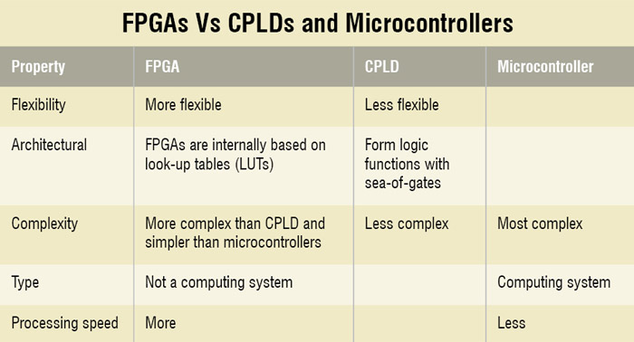
The primary differences between CPLD and FPGA are architectural. A CPLD has a restrictive structure which results in less flexibility. The FPGA architecture is dominated by interconnects, which makes them not only far more flexible but also far more complex to design.
One major difference between the FPGA and CPLD architectures is that FPGAs are based on look-up tables while CPLDs form the logic functions with sea-of-gates.

FPGA vs Microcontroller
A microcontroller is an integrated circuit chip that is often part of an embedded system. It is a small computer on a single integrated circuit containing a processor core, memory, and programmable input/output peripherals. A microcontroller differs from a microprocessor, which is a general-purpose chip that is used to create a multi-function computer or device and requires multiple chips to handle various tasks.
A microcontroller is a computing system. It has lots of hierarchical rules and commands over its input and output. It has its own processing unit. On the contrary, FPGA is not a computing system.
FPGAs are used for simpler operations, but they have higher processing speeds than microcontrollers. The important points mentioned above are summarised in the table above.
Also, find out the differences between a microcontroller and a microprocessor
Advantages
FPGAs offer a range of advantages, including:
Long-time availability
FPGAs enable you to make yourself independent from component manufacturers and distributors since the functionality is not given by the device but its configuration. The configuration can be programmed to be portable between miscellaneous FPGAs without any adaptation.
Can be updated and upgraded at your customer’s site. FPGAs, in contrast to traditional computer chips, are completely configurable. Updates and feature enhancement can be carried out even after delivery at your customer’s site.
Fast and efficient systems
Available standard components address a broad user group and consequently often constitute a compromise between performance and compatibility. With FPGAs, systems can be developed that are exactly customised for the designated task and are therefore highly efficient.
Performance gain for software application
Complex tasks are often handled through software implementations in combination with high-performance processors. In this case, FPGAs provide a competitive alternative, which by means of parallelisation and customisation for the specific task even establishes an additional performance gain.
Real-time applications
FPGAs are perfectly suitable for applications in time-critical systems. In contrast to software-based solutions with real-time operating systems, FPGAs provide real deterministic behaviour. By means of the featured flexibility, even complex computations can be executed in extremely short periods.
Massively parallel data processing
The amount of data in contemporary systems is ever increasing, which leads to the problem that systems working sequentially are no longer able to process the data on time. Especially by means of parallelisation, FPGAs provide a solution to this problem.
Tool support
FPGA design flows support the use of third-party EDA tools to perform design flow tasks such as static timing analysis, formal verification, and RTL and gate-level simulation.
Disadvantages
One major disadvantage of FPGAs is the relatively large propagation delays. To complicate things, these delays are hard to predict before the circuit design is finished. This is due to the need to route signals through multiple levels of logic and interconnection blocks. Typical RAM-based FPGA circuits will have propagation delays of 20 to 50 ns.
Another disadvantage of FPGAs is the expensive and slow design software. FPGAs are typically designed using either schematic capture or HDLs. This is typically done with third-party tools like Viewlogic schematic capture. These tools then output netlists (lists of gates or cells and how these are to be logically interconnected). The components in the netlist must then be assigned to specific cells on the device and the routing between cells laid out. This place-and-route process is a complex optimisation problem which typically includes constraints on propagation delay and the number of cells used.
Also, with FPGAs, there is the least efficient use of silicon/wiring resources.
The advantages, however, far outweigh the disadvantages, and hence FPGAs are widely used.
The article was originally published in November 2015 and has recently been updated.


send me FGPA progaming video for how to use