


The ability to tune properties of a layered material by varying the twist angle provides the possibility for a single material to perform a variety of functions instead of using many materials for different functions.
Tunability of a material’s properties has always been at the core of material research and development, and scientists are exploring options to find ways of tuning the properties to desired levels, including by doping, stretching, compressing and now twisting. Twisting single-atom layers of graphene and other substances has already shown interesting properties in the past. As an example, here electrons no longer jump from one atom to the next, but tend to flow over the surface of the sheet, called plasmonics.

Plasmonics is being considered in various ways; one of this being the very low resistance involved in flow of electrons and in the interaction happening in the tera-hertz range (optoelectronics). Researchers are always looking at emerging properties when two layers of graphene and other substances, each one a single atom thick, are layered on top of one another at different angles.
In this direction, twistronics is the study of how the angle (twist) between layers of 2D materials can change their electrical, optical and mechanical properties. Such materials as graphene have shown to have vastly different electrical properties (ranging from non-conductive to superconductive) depending on angle between the layers.
With the magic angle of twist, scientists have reported evidence of a new kind of quantum optical behaviour in similar twist-tunable stacks of other types of 2D materials. It turns out moiré effects can be obscured somewhat by an imperfect moiré pattern, which will lead to light emission similar to defects, and excess laser excitation power, which will provide a broad background.

The science and engineering behind twistronics
Achieving a variety of electronic properties in conventional materials normally requires changing their chemical composition by doping technique. Researchers in recent times have realised that weak coupling between different layers of 2D materials can be used to control these materials in ways that were not possible with more conventional structures.
One unique example in this direction is the ability to tune electronic properties of 2D-layered graphene by varying angle between the layers by twisting. Thus, ability to vary electronic properties of a 2D material just by altering the twist angle between its layers is therefore a fundamentally new direction in device engineering.
Until now, researchers needed to make a whole new device for each different twist angle, which often involved fabricating a large number of devices. This also made it difficult to resolve angle-dependent effects independent of sample-to-sample variations. Many interesting angle-dependent characteristics (such as superconductivity in twisted bilayer graphene) could only be observed within a very narrow range of the target angle.
Researchers have now succeeded in making a single device whose layers can continuously rotate locally while measuring its physical and electronic properties. This new platform allows switching between an arbitrary number of complementary states in the device.
Researchers at Columbia University, USA, have developed a new device structure to make it possible to vary the twist angle between layers of 2D materials and to investigate how this angle affects electronic, optical and mechanical properties of the material.
Measurements carried out on a single structure with twisting rather than multiple ones—as was the case before—could advance the emerging field of twistronics as a fundamentally new approach to device engineering.
For instance, graphene, a 2D sheet of carbon atoms, normally does not have a band gap, but it develops one when placed in contact with another 2D material, boron-nitride, with a hexagonal structure. Both these materials have closely matching lattice constants, and layers of graphene and boron-nitride form a large moiré superlattice. Then, by twisting the layers so that they become misaligned and angle between them becomes large, the band gap disappears. Simply varying the angle between 2D material layers, thus, means that graphene can be tuned from metallic to semiconducting.
Researchers at Massachusetts Institute of Technology (MIT), USA, have recently discovered that placing two layers of graphene together, when rotated relative to one another at the magic angle of 1.1, turns the normally metallic material into a superconductor.
Basics of the technique
This technique takes advantage of low interfacial friction that naturally exists between layered 2D materials, and also absence of strong chemical binding between the layers so they slide over one another easily. In the fabrication process, researchers studied graphene/boron-nitride heterostructures and designed a device in the shape of a gear that was intentionally made so that it was rotatable. Previously-developed techniques were employed to mechanically pick up this nano-sized gear (made of boron-nitride) and place it over the top of the active area (graphene).
Once in place, they used an atomic force microscope to push along one tooth of the gear, causing it to rotate. This shows that we can achieve and control rotation in graphene/boron-nitride heterostructures, and can dynamically vary electrical, optical and even mechanical properties of a device made from these structures. It is, thus, demonstrated that energy gap observed in graphene is tunable and can be turned on or off as per requirement just by changing the twist angle between the layers. Further spectroscopic studies of twisted bilayer graphene have revealed strong electron-electron correlations at the magic angle.
It is already known that graphene can conduct electricity at ultra-high speed, but researchers took a giant leap by turning graphene into a superconductor—a material that allows electricity to flow without resistance. This was achieved by placing one sheet of graphene over another and rotating the other sheet to a special orientation, or magic angle, and cooling the ensemble to a temperature of 1.7K. The twist radically changed the bilayer’s properties—turning it first into an insulator and then, with application of a stronger electric field, into a superconductor.
Role of magic angle in twistronics
Research has proven that magic angles are real. Physicists are trying to apply the twistronics approach to other configurations of graphene. Researchers have been experimenting with twisting two layers of graphene and have found evidence of superconductivity and correlated physics. Others are stacking up three or more layers of graphene in the hopes of gaining superconductivity at other magic angles, or perhaps even when they are aligned. Physicists point out that higher layer stacking may lead to superconductivity temperature to climb.
Other magic angles may play a role, too. Some groups are squeezing sheets of graphene more tightly together to increase the magic angle, making it easier to achieve, and other materials are also coming into the fold of twistronics.
Semiconductors and transitional metals can be deposited in twisted layers, and are seen as good candidates for correlated physics—perhaps, better than twisted bilayer graphene.
Researchers are thinking of hundreds of materials that can be manipulated this way in the hope of boosting correlated effects in magic angle twisted bilayer graphene devices by literally smoothing out the wrinkles in their fabrication.
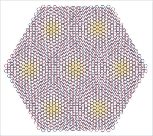
Because there is no chemical bonding between the two layers, and because slightly offset layers try to settle into alignment, forcing them to hold a magic angle twist creates stresses that lead to sub-microscopic hills, valleys and bends. Those local distortions mean that some regions of the device might be within the magic range of twist angles, while other regions are not.
Development towards twistronics
In 2007, National University of Singapore physicist Antonio Castro Neto hypothesised that pressing two misaligned graphene sheets together might yield new electrical properties, and separately proposed that graphene might offer a route to superconductivity, but he did not combine the two ideas.
The theoretical basis of twistronics was further developed by Allan MacDonald in 2011 by predicting that a specific magic angle would radically change the amount of energy a free electron would require to tunnel between two graphene sheets. This hypothesis was confirmed by Pablo Jarillo-Herrero and his student Yuan Cao of MIT and colleagues from Harvard and National Institute for Materials Science in Tsukuba, Japan. They verified in 2018 that superconductivity existed in bilayer graphene where one layer was rotated by an angle of 1.1 relative to the other, forming a moiré pattern, at a temperature of 1.7K.
They created two bilayer devices that acted as an insulator instead of a conductor under a magnetic field; increased field strength turned the second device into a superconductor. Because the only variable is field strength, studying superconductivity in bilayer graphene is faster and more convenient than working with multi-element cuprate crystals.
Experiments have also been done using combinations of graphene layers with other materials that form heterostructures in the form of atomically-thin sheets that are held together by the weak Van der Waals force. A study in July 2019 found that, with addition of a boron-nitride lattice between two graphene sheets, unique orbital ferromagnetic effects were produced at a 1.17 angle, which could be used to implement memory in quantum computers.
Applications
Twistronics is an approach to device engineering in which twist angle between layers of 2D materials such as graphene affects their electronic, optical and mechanical properties. Future applications can be summarised as:
- It will help in the development of new kinds of switching technologies, for example, tunable sensors and tunable electro-mechanical and electro-optical-based devices.
- Though single layers of graphene do not superconduct on their own, they exhibit superconductivity in twisted bilayer resulting from the interaction between layers. This will lead to various applications of superconducting graphene.
- Researchers believe that it might be possible to introduce, and turn on and off, similar effects, such as spontaneous magnetic ordering and topologically-protected band gaps, with controlled twisting. Results using engineered artificial excitonic crystals of Van der Waals heterostructures highlight the possibility of their applications in nano-photonics and quantum information.
- The work has fundamental significance, providing an attractive platform from which to explore and control excited states of matter, such as topological excitons and a correlated exciton Hubbard model, in transition metal dichalcogenides.
Future scope
Misaligned stacks of 2D materials on twisting are exhibiting different curious properties, and twistronics is gaining steam and interest of many research teams around the world. It is expanding to include other types of materials beyond graphene. The result does not mean getting superconductivity at ambient temperature and to use it in everyday applications.
The property is seen at the very nano-metric level, but what makes it interesting for physicists is that it can open a path to understand superconductivity, and that understanding may open up practical approaches towards usable ambient temperature superconductivity. The ability to tune properties of a layered material by varying the twist angle provides the possibility for a single material to perform a variety of functions instead of using many materials for different functions.
Presently, electronic circuits are built from a finite number of components including metallic conductors, insulators, semiconductors and magnetic materials, and this process requires integration of a variety of different materials, posing significant engineering challenges. But single materials exhibiting a change of properties with twisting can be used to realise each of these components, enabling significant new engineering opportunities.
Dr S.S. Verma is a professor at Department of Physics, Sant Longowal Institute of Engineering and Technology, Sangrur, Punjab
