


ANSYS is leveraging its 3D-IC design technology simulation software to transform chip integration by enhancing performance, reducing power consumption, and shrinking form factors for next-generation devices. Marc Swinnen, Director of Product Marketing, discusses the impact of thermal management on stacking density in multi-die systems with EFY. Read on…

Q. What is Ansys RHSC ET, and what does it offer regarding semiconductor chip-package-system design?
A. Ansys RedHawk-SC Electrothermal (RHSC ET) is a verification product designed to analyse 2.5D/3D-IC multi-die semiconductor configurations. These systems typically involve chiplets and HBMs on an interposer or substrate within a package enclosure. It conducts thermal, power, signal, and structural integrity analyses on the system.
It can collaborate with other Electronic Design Automation (EDA) tools to analyse chips at different scales, from nanometres to millimetres to meters, ensuring comprehensive system understanding. RHSC ET facilitates multi-scale analysis across various physics domains, from prototyping to manufacturing signoff. It manages a set of Reduced Order Models (ROMs) available in the Ansys platform, including chip power, thermal, signal, and electrostatic discharge models. RHSC ET performs assembly and full-system analysis using these models, incorporating factors like heatsinks and fluid dynamics simulations.
Q. What are the key industry trends and emerging challenges in thermal simulation for 3D-IC designs?
A. While most multi-die designs today are implemented as 2.5D designs, there is a clear desire for the higher integration densities achievable with 3D stacking technology. The primary obstacle to this development is thermal management. Cooling 3D assemblies is inherently more challenging. Innovative techniques, such as dedicated thermal-spreader layers in the metal stack, are being developed, along with advanced cooling methods, including liquid cooling.
This is accompanied by a corresponding emphasis on reducing heat production. Low power design is now a significant concern, even for products not reliant on battery power.
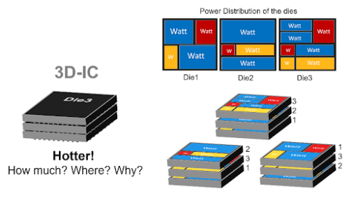
3D-IC design has elevated thermal analysis to a top-level design parameter during prototyping, rather than solely at the packaging stage, to prevent overheating issues. When planning a multi-die layout, understanding which chiplets generate heat and when they do so is crucial. Placing two chiplets next to each other that happen to heat up simultaneously can jeopardise the entire design.
Q. How does the RHSC ET software account for the stacking of multiple layers and their impact on thermal management?
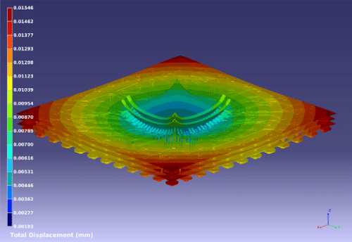
A. Thermal management is the fundamental constraint on maximum integration density or how small a system can be. A single high-performance chip can easily consume 100W to 200W. Cooling cannot exceed a certain power density limit, resulting in thermal runaway, parameter drift, mechanical warping, or melting when stacking multiple components near or on top of each other.
The Ansys platform offers tools that simulate the three core aspects of thermal management: power/heat generation, heat conduction, and heat dissipation.
Heat is generated in silicon chips based on their activity and power supply currents, captured by our chip thermal models (CTMs). The software models heat conduction and distribution throughout a 3D-IC setup using CTMs for each chip, interposer, and package. Ansys meshing and thermal conduction simulators illustrate heat flow over time. The final temperature relies on effective heat dissipation through system-level elements such as heat sinks, thermal spreaders, and cooling fans. This system-level simulation also employs other software to model heat-sink and air flow using computational fluid dynamics (CFD) simulation.
Q. How user-friendly is the software for engineers and designers who are not experts in thermal analysis?
A. Thermal analysis is well-established for Ansys but relatively new for most 2.5D/3D-IC silicon designers. Historically, thermal concerns were often addressed later in the package design process, but they are now integral from the prototyping phase. Many companies struggle to coordinate expertise across various teams – chip, package, and system PCB. These teams encounter difficulties in aligning their efforts due to the interconnected nature of 3D-IC design.
The purpose of Electronic Design Automation (EDA) tools is to simplify technology applications. Our software streamlines the application of Ansys’s simulation and meshing engines to 3D-ICs, especially for new users. Given the evolving 3D technology landscape and the absence of standard workflows, flexibility is vital to accommodate diverse customer approaches.
Q. Please share insights into thermal simulation software adoption rates for 3D-IC designs across different industries.
A. The primary adopters of multi-die design include:
- High-capacity memory manufacturers: The vast majority now employ multi-die stacks known as ‘high bandwidth memory’ (HBM).
- High-performance computing (HPC) market: Most high-end microprocessors, mobile application processors, and graphic processors are designed as 2.5D implementations.
- Image sensor manufacturers: CMOS image sensors (CIS) in most digital camera systems are exploring 3D stacking of the sensor with image processing logic.
Q. What insights does the software provide for optimising power delivery and reducing power-related issues?
A. From real-world software impact to ambient heat dynamics, RHSC ET charts a course towards efficiency and reliability in 3D-IC design.
- Real-World Software Impact: RHSC ET accounts for the thermal effects of running actual software applications on the 3D-IC stack, using activity sets from real software apps, often obtained from hardware emulators. This approach is essential for reliable thermal analysis.
- Mechanical Warpage and Stresses: The tool simulates mechanical warpage and stresses in the multi-die stack caused by differential thermal expansion. These stresses can impact system reliability and lifespan, potentially leading to microbump cracking and functional errors due to changes in transistor parameters.
- Material Influence on Thermal Conduction: The thermal conduction in a component stack is influenced by material properties. Our software interfaces with a materials database system, allowing designers to experiment with different materials to find the optimal combination considering thermal and electrical properties.
- Ambient Heat Impact: The tool also considers the impact of ambient heat on system performance. For instance, ambient temperature variations can affect the electronic assembly if the 3D-IC assembly is positioned near a car engine with fluctuating temperatures.
These capabilities are invaluable for accurate and comprehensive thermal analysis.
Q. What do you mean by electromigration reliability? How does RHSC ET technology assess and predict electromigration reliability in 3D-IC designs?
A. Electromigration is a physical effect where a strong electrical current physically moves metal atoms in a wire, akin to a strong river current moving rocks downstream. This metal migration results in ‘voids’ (missing metal that has migrated away) and ‘hillocks’ (accumulations of metal that have moved upstream) in chip interconnects. Electromigration is a relatively slow process that can take months or even years to manifest as a problem. Therefore, it cannot be detected by testing during the manufacturing stage, but rather through proper design practices.
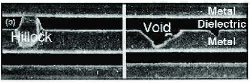
The silicon foundries (manufacturing plants) specify a maximum allowable current for a given wire cross-section that cannot be exceeded. RedHawk-SC and Totem can verify the current through every one of the billions of polygons that make up a chip’s interconnect, flagging any violations before manufacturing. Solving electromigration issues entails widening wires, reducing current, or both.
Electromigration is a concern wherever large currents pass through very thin wires. This is primarily an on-chip issue, but modern 2.5D/3D-IC interconnects, especially on silicon interposers connecting multiple dies, have become so thin that it is also a concern for 3D-IC assemblies.
Q. How does the software address coupling effect challenges in 2.5D and 3D IC systems?
A. The market offers numerous multi-die technologies from all major foundries. 3D-IC strictly refers to vertically stacked dies, while 2.5D refers to side-by-side die placement on an interposer. Although most designs today are technically 2.5D assemblies, they typically include 3D HBM (high bandwidth memory) stacks. To simplify matters, “3D-IC” is often used as an umbrella term for all these technologies.
RHSC ET handles both 2.5D and 3D technology options adeptly. Thermal effects are more pronounced in 3D stacking than in 2.5D, but the same software is used to analyse both.
Q. How does the software manage the computational demands of large-scale multiphysics simulations for 2.5D/3D-IC systems?
A. A single die in a 2.5D/3D-IC system contains billions of transistors, and multi-die setups consist of multiple dies, interposer layers, through-silicon-vias (TSVs), and microbump connections. Two approaches handle this data complexity in multi-die systems:
Extensive use of cloud computing – Our cloud-optimised elastic compute data infrastructure, SeaScape, enables detailed analysis of full chips.
Hierarchical modelling with Reduced Order Models (ROMs) – These models capture key physical effects accurately, enabling comprehensive system-level analysis while minimising data requirements. ROMs cover chip power, thermal, signal, electrostatic discharge models, interposer and package behaviour. They are applied in system-level analysis at the board level as well.
Q. How does the software handle modelling heterogeneous systems with multiple dies, interposers, packages, and PCBs? What level of detail can it achieve?
A. The recommended approach for comprehensive heterogeneous full-system analysis using RHSC ET is hierarchical modelling with Reduced Order Models (ROMs). These models provide sufficient detail for system-level analysis while minimising data requirements. ROMs encompass major physical effects, such as chip power, thermal, signal, and electrostatic discharge models.
Each ROM is generated from a detailed signoff analysis of individual elements like chiplets, interposers, and packages, using appropriate tools such as RedHawk-SC, Totem, and RaptorX.
RHSC ET combines ROMs to analyse the entire 2.5D/3D stack. It can even use a mix of ROMs and full-data models to achieve accuracy versus runtime trade-offs. Icepak employs ROMs to compute PCB-level thermal conditions (heatsinks, fans), while SIwave uses them for PCB-level EM/IR analysis.
Q. What challenges does the model encounter in creating accurate physical models and verifying their connectivity?
A. The challenge in creating ROMs lies in balancing interior visibility with data size. For optimisation purposes, designers may want to identify internal ROM details linked to top-level system issues. This is possible but reduces the data reduction achieved by the ROM.
Regarding connectivity, RHSC ET is a multiphysics analysis platform that integrates with popular physical design tools (e.g., 3DIC Compiler from Synopsys). These design tools primarily ensure correct connectivity through the multi-die stack.
