New vertical device architecture promises stable, ultra-dense semiconductor stacking for future AI and high-performance electronics.
Researchers have developed a new transistor architecture designed to support the next generation of 3D stacked semiconductors, addressing one of the biggest challenges in ultra-dense chip design—current leakage. The innovation could enable more efficient processors for AI, high-performance computing, and advanced electronics.
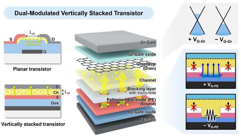
A research team led by scientists at the Daegu Gyeongbuk Institute of Science and Technology (DGIST) introduced a dual-modulated vertically stacked transistor that maintains stable operation even at nanoscale dimensions. The design incorporates a dual-gate structure that improves control over the channel and suppresses unwanted current leakage—an issue that becomes more severe as transistors shrink and are stacked vertically.
3D semiconductor architectures are increasingly viewed as a key pathway for continuing performance improvements as traditional transistor scaling approaches physical limits. Instead of only shrinking components in two dimensions, engineers stack devices vertically to dramatically increase transistor density and computational power within the same chip footprint. However, vertically stacked transistors typically face reliability problems. Leakage currents, unstable switching behavior, and complex electrostatic interactions often degrade device performance, limiting the practicality of large-scale 3D integration.
The DGIST team addressed these challenges using a sandwich-like transistor configuration with dual-modulated gates. This structure enhances electrostatic control over the channel and ensures stable operation even when devices are stacked in multiple layers. According to the researchers, the approach overcomes key limitations of conventional vertical transistor designs.

The technology could play a crucial role in future chip architectures where logic devices are stacked layer by layer to increase performance without expanding chip size. Such designs are particularly attractive for AI accelerators, data-center processors, and energy-efficient mobile electronics, where higher density and lower power consumption are essential.
Researchers say the new device architecture may serve as a foundational building block for highly integrated 3D semiconductor systems. If successfully commercialized, it could accelerate the transition toward vertically integrated logic chips—one of the semiconductor industry’s most promising strategies for sustaining performance growth in the post-Moore’s-law era.