


An optical AI chip processes light directly, uses less power, supports different vision tasks, and can be made in about 15 minutes.
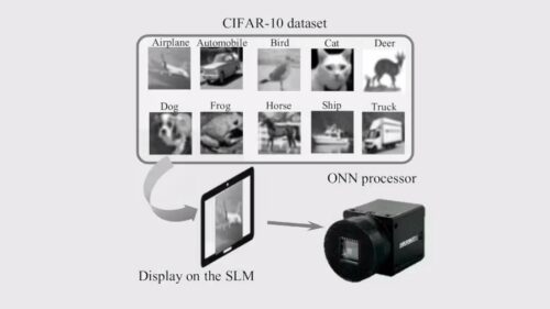
Researchers from the Chinese University of Hong Kong and the Center for Perceptual and Interactive Intelligence have developed a new way to build ultra-low-power machine vision systems for embedded cameras. Their approach uses a task-agnostic optical neural network that can be fabricated into a chip in about 15 minutes.
Instead of converting light into electrical signals before processing, the optical neural network processes incoming light directly. This allows image processing at the speed of light while using much less power than conventional electronic systems. However, building such optical systems has been difficult because they require millions of tiny optical components that are only a few hundred nanometres in size.
To address this, the researchers used a two-photon lithography (TPL) holographic light-field control system with a parallel scanning method. The technique produced a millimetre-scale optical neural network containing four million optical neurons, each measuring about 500 nanometres, in just 15 minutes.
Unlike many existing optical neural networks that are designed for a single application, the new chip is task-agnostic. It acts as a general optical encoder, while different machine vision tasks are handled by retraining a small digital neural network with as few as 1,000 weights. This means the same optical chip can be reused for multiple applications without changing its hardware.
The researchers tested the prototype on several machine vision tasks, including handwritten digit recognition, cell classification, human action recognition and facial key-point detection. The system achieved classification accuracy between 97% and 99%.
According to the researchers, the fabrication method is suitable for both rapid prototyping and large-scale manufacturing. They say it is compatible with existing ultraviolet nanoimprint systems, making it possible to produce optical neural network chips at lower cost than many current approaches.
The team also believes the technology can be expanded further. By using different materials and nanoimprint replication techniques, future versions could operate across wavelengths ranging from near-ultraviolet to infrared. They also suggest that larger, centimetre-scale optical chips could be manufactured using tiled writing and imprint replication for practical imaging applications.