





The new architecture integrates power devices directly into a silicon wafer, targeting smaller, cooler, and more efficient power systems for AI infrastructure, EVs, and industrial equipment.
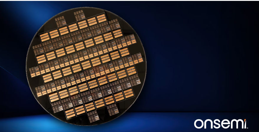
onsemi has introduced the Embedded Power Platform (EPP), a new power-device integration and packaging architecture designed to address the growing need for compact, thermally efficient power delivery in AI infrastructure, electric vehicles, and industrial systems. Unlike a conventional discrete product, EPP is a platform rather than a single IC or model-numbered device; therefore, no specific IC/model number has been assigned to the technology.
The architecture uses the silicon wafer itself as the package, allowing multiple semiconductor dies to be integrated within a common wafer-level structure. Power switches, drivers, controllers and isolation functions can be combined in the same architecture, while supporting silicon, silicon carbide (SiC), gallium nitride (GaN) and future semiconductor technologies. This approach allows electrical, mechanical, and thermal characteristics to be considered together instead of being optimized separately.
A key benefit is increased power density. Depending on the application, it is designed to deliver up to 3–5 times higher power density than conventional approaches. The architecture can also reduce electrical losses through lower parasitic inductance and provide improved heat dissipation by using the platform footprint as part of the thermal path. These characteristics are particularly relevant to AI systems, where increasing rack power is placing greater pressure on space and cooling capacity.
The key features are:
- 12-inch wafer-based manufacturing approach
- Silicon, SiC, and GaN technology agnostic
- Wafer-level redistribution layer architecture
- Integrated power, control, and isolation functions
- Electrical, thermal, and mechanical co-optimization
The platform also replaces conventional wire-bond connections with wafer-level redistribution layers (RDLs). This reduces parasitic effects and supports tighter electrical integration between the semiconductor dies. By bringing semiconductor manufacturing techniques into system-level power integration, the architecture is intended to reduce design iterations and accelerate development, with development cycles potentially reaching about four months.
For AI infrastructure, the technology can enable more compact power-conversion and protection hardware. In an early solid-state circuit-breaker design, an EPP-based implementation was approximately 50% smaller and 20% cooler than an existing design. For EV traction inverters, the platform is designed to deliver up to 4x higher power density and 15% lower power losses, supporting smaller and lighter inverter architectures. The same architecture can extend to EV charging, renewable-energy converters, energy-storage systems, and industrial automation, where higher power must increasingly fit into smaller system footprints.
Click here for the original announcement.
