


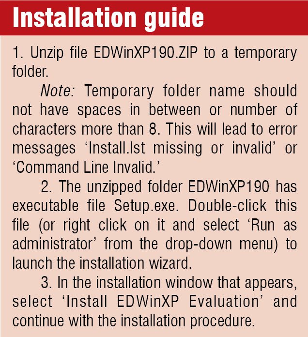
EDWinXP is an integration of tools that cover all stages of electronic design process, which include schematic capture, circuit simulation, PCB design and layout, generation of PCB manufacturing and testing documentation. It also provides the users with several verification and validation tools to check the integrity and correctness of the schematic and PCB layout design. One can use this suite to produce PCBs of several kinds including flexible PCBs, RF boards and multi-layer PCBs.
One of the most notable benefits of using this tool is that you can perform reverse engineering of designs. This means, project database can be completely reconstructed using full set of artworks in Gerber ASCII format or complicated PCB Outline. This is achieved through two stages. First stage involves import of graphic elements in artworks and distribution into relevant categories. As an example, the traces are distributed to Trace Master and pads to Padstock category. Next stage of reconstruction has several steps executed in a predefined sequence.

The inclusion of IPC-355 format for PCB assembly output and IPC-356A format for bare board testing allows PCB manufacturers to verify Gerber data against the design net list. This would assist in identifying several design flaws which might have resulted in unusable PCBs.
 Fast, round the clock support by the company is another major benefit of using this software. This company is based in India and works very closely with its customers. The users can even give suggestions and influence the development of this tool by participating in the active discussion forums at company’s website.
Integrated tools
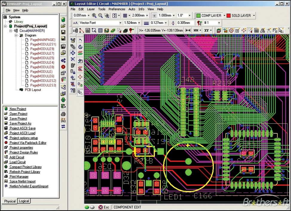
The seamless integration of tools in EDWinXP makes it a bit complicated to start with but, once mastered, this package is easy to work with. Its graphical user interface (GUI) is simple to follow and allows easy shifting from one tool to the other in the package. The suite has following components integrated into the main software tool.
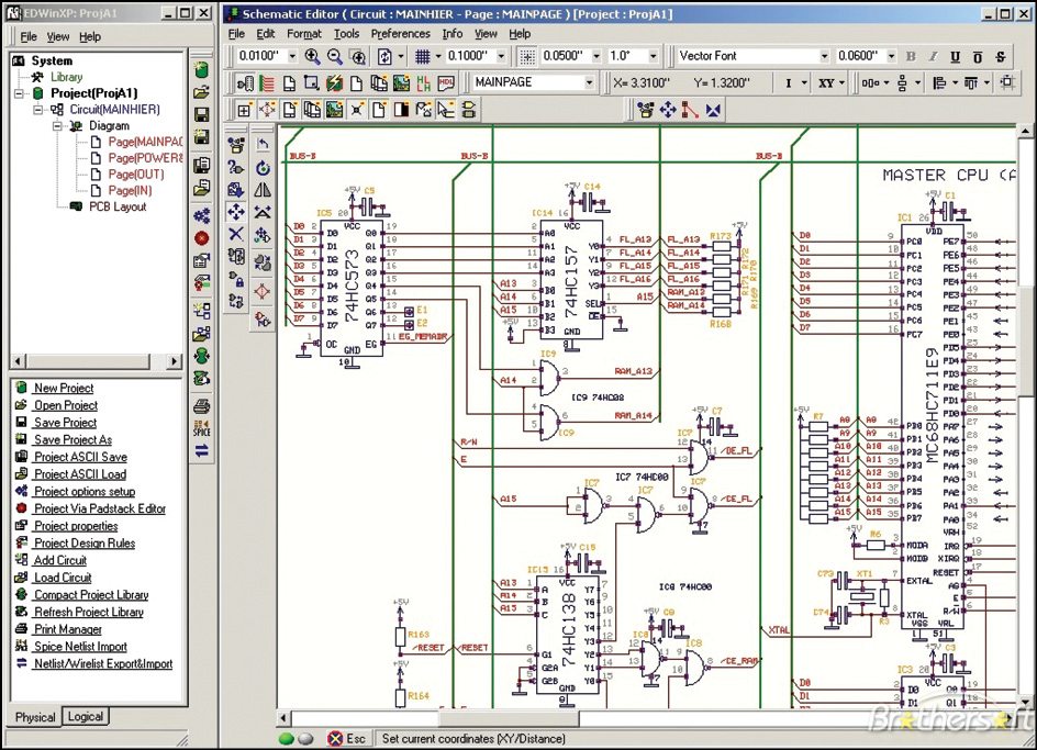
Schematic Editor. It is the front end of any PCB design for creating circuit diagrams using standard symbols and connections. Each component in the schematic has a label that displays parameters of that particular component. You can also modify or add other parameters or texts and notes to it. This captured schematic is automatically front annotated to layout mode by the tool. Schematic DXF Export option lets you export EDWinXP schematic graphics into AutoCAD DXF format.
Library Editor. EDWinXP library comes with a large collection of predefined graphical representations of standard components in both schematic and PCB layout view. The user can update, customise or enhance the components of the library using the Library Editor tool. The components also contain details like packaging information, thermal parameters and link to simulation modules.
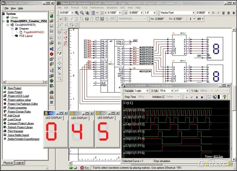
Mixed Mode and EDSpice simulators. Simulators let you test the performance of a circuit for various DC operating points for a range-applied signal over output levels, supply voltages and temperatures. EDWinXP provides a Mixed Mode Simulator (the system’s native circuit level analyser) and an EDSpice Simulator (full implementation of SPICE standards).
 Layout Editor. This lets you create and edit PCB layout for the designed schematic. It also allows you to begin layout with a pre-existing schematic, edit existing layouts or capture the design directly in PCB layout mode. Operations like placing components, renumbering of components, routing and error check are automated. 3D Board Viewer and 3D Trace Viewer are the other features.
Fabrication Output Manager. This program is used to generate manufacturing output files for Photoplotter, NC Drill, etc. NC Drill data can be generated in Excellon format with or without tool movement optimisation. Users also have the option to create drill templates that can be printed or saved in Gerber format for photoplotting. It is possible to insert dimensions of various mechanical drawings. PCB assembly output is generated in IPC-355 format and bare board testing output is obtained in IPC-356A format. You can also export the entire database in GenCAM format. Users can generate disk files containing bill of material and generic data for pick-and-place machines. The tool supports RS-274D and extended RS-274X Gerber ASCII formats. Integrated Gerber ASCII file viewer enables the user to verify artworks before sending them for plotting and manufacturing.
Features
EDWinXP is rich in features and the added features in each revised version are incorporated from the customers’ feedback and suggestions. The key features are:
Front and back annotate. Designs can be captured in Schematic Capture or Layout Editor. The design created using Layout Editor is back annotated to the Schematic Editor and the one created using Schematic Editor is front annotated to the Layout Editor.
Microcontroller kit. It comes with a microcontroller kit that mimics the functionality of 8051, AVR, PIC and Motorola microcontrollers. Moreover, editing and compilation of programs in C and Assembly languages and debugging the code in real time is possible. The kit also contains series of models like memory, 7-segment displays, series/parallel pattern generators and interrupt generators for generating parallel and serial data patterns and asynchronous hardware interrupts.
 Filter designer. EDWinXP offers automated filter designing where you can choose the filter type, enter the output frequency and quality range, and the program calculates the parameters and generates schematic. This can be imported to PCB layout format.
Autoplacing and autorouting. Autoplacing of components in the schematic layout is possible with Schematic Editor. The autoplacing parameters and design rules can be set by the customer. Autorouter can be executed in PCB layout with default parameters or user-defined parameters using Arizona Autorouter in EDWinXP.
Analysers. Another feature is the different types of analysers that help a user check the integrity and correctness of layout design. The electromagnetic analysers—field analyser and signal integrity analyser—are used to inspect electromagnetic effect on the board, and thermal analyser lets you examine the thermal hotspots on the board.
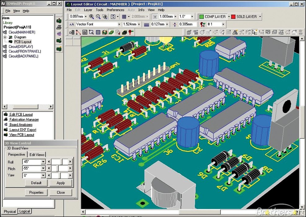
And much more! EDWinXP has option to get a 3D view of the component packages. VHDL Editor lets you automate project creation from VHDL source. With the project version control you can keep track of the changes made to the projects. The entire design details are stored in an integrated database that can be accessed simultaneously by the Schematic Editor, Layout Editor, Simulators and Fabrication Manager. This program offers backward compatibility to older DOS-based design files. VHDL/Truth Table to diagram converter, 3D IDF file viewer, Filter Designer, ODB++ export and import are some of the other modules available on EDWinXP.
Different types of licensing
The evaluation version of EDWinXP provided in the DVD comes with all the features of EDWinXP with 14-day licence, after which it can be activated directly from Visionics website www.visionics.a.se or through their distributors. Upgrades can be made to Non Commercial, Commercial and Small Biz versions of EDWinXP Schematic, Standard, Deluxe or Professional packages.
Online technical support for the product and for creating libraries is available or Besides, Visionics offers live chat for customers with the support desk, thereby ensuring quick response and solution to design issues. Service pack updates containing additional features and bug fixes are posted on the website. The site also provides discussion forums on the product, newsletters and elaborate tutorials, training projects and demos in document and/or video formats.
Download latest version of the software: click here
The author is a technical correspondent at EFY
