


 Sometimes a simple analogue power supply with adjustable output voltage and adjustable current-limiting function is needed. This article presents a simple power supply using an adjustable regulator LM350 that provides variable output up to 17V and maximum output current below 2A. LM350 has higher power dissipation as compared to commonly-available adjustable voltage regulator LM317 and, hence, has higher guaranteed output current. This power supply may be useful in laboratories and for hobby projects.
The circuit diagram of the power supply is shown in Fig. 1. It is built around bridge rectifier (BR1), adjustable voltage regulator LM350 (IC1), transistors BC327(T1) and BC337(T2), and a few other components.
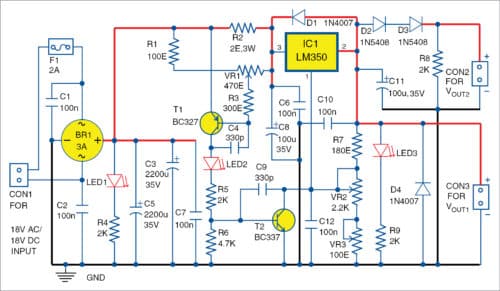
Input to connector CON1 can be AC or DC. If you use an 18 to 20Vrms transformer with 2A current ratings, you can have output voltage VOUT1 from 1.2V up to around 16.5V available at CON3, and VOUT2 from 0V to 15V available at CON2. Input is protected with 2A fuse F1. Capacitors C3 and C5 (2200µF) are the main filtering capacitors.
Input voltage is limited by maximum input voltage of IC LM350. Maximum power dissipation of LM350 is around 25W.
According to the data sheet, input voltage of LM350 can be from around 4.5V to 35V, and output voltage can be adjusted from 1.2V to 33V; however, we need output voltage lower than 17V.

Output voltage VOUT1 can be calculated using the following relationship:
VOUT1=1.25V (1+(VR2+VR3)/R7))
Output voltage VOUT2 is around 1.5V lower than VOUT1, and can consequently start from 0V.
Transistors T1 and T2 are implemented for adjustable current-limiting function along with potentiometer VR3. The Minimum output current is around 0.35A, and depends on resistors R2 and VR3.
Wiper of VR3 should be at the right-most position to get minimum output current, and at the left-most position for maximum output current. The maximum output current is around 2A. When VR1 is adjusted for maximum output current, T1 and T2 will be on, and LED2 will glow. Otherwise, T1 and T2 will be off, and the LED2 will also be off.
Capacitors C4 and C9 prevent oscillations of T1 and T2 during transitional phases. The output voltage is adjusted with VR1 and VR3. VR2 is used for coarse adjustment, while VR3 is used for more precise output voltage adjustment.
Construction and testing
A PCB layout for this power supply circuit is shown in Fig. 2 and its component layout in Fig. 3. Assemble the circuit on the designed PCB or veroboard. Connect around 18 to 20Vrms input to CON1. Glowing of LED1 indicates the presence of power supply in the circuit. LED2 glows when higher current is taken from the load. LED3 glows when outputs are available at CON2 and CON3.
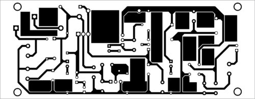
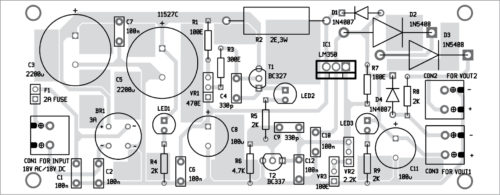
For downloading PCB and component layout PDFs: click here
Measure outputs across CON2 and CON3 using a voltmeter. You should be able to get output voltage VOUT1 from 1.2V up to around 16.5V, and VOUT2 from 0V to 15V depending on positions of VR2 and VR3.
Petre Tzv Petrov was a researcher and assistant professor in Technical University of Sofia, Bulgaria and expert – lecturer in OFPPT (Casablanca), Kingdom of Morocco. Now he is working as an electronics engineer in the private sector in Bulgaria
Will try this one.
Best of luck