




A two-channel analogue front end supports high bandwidth, adjustable gain, selectable input impedance and signal conditioning for data acquisition.
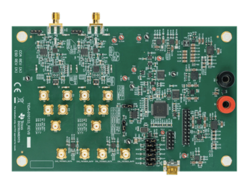
High-bandwidth data acquisition systems such as digital storage oscilloscopes require an analogue front end that can handle a wide range of signals while maintaining signal quality. Texas Instruments’ reference design provides a two-channel analogue front end with DC to 500MHz bandwidth and selectable 50Ω or 1MΩ input impedance.
The design is intended for benchtop digital storage oscilloscopes, digitisers operating at 50MSPS or higher, and precision multifunction input and output data acquisition systems. It supports AC or DC coupling and provides up to 40dB of programmable gain. The reference design also includes trigger functionality, precision digital-to-analogue conversion for offset and common-mode control, and an SMA connector for connection to a high-speed analogue-to-digital converter evaluation module.
At the input, the design uses a high-impedance buffer with a junction-gate field-effect transistor input stage. The buffer can operate in a composite loop with a precision amplifier. This approach combines the DC precision of the low-frequency path with the wide large-signal bandwidth of the high-frequency path. The input can be configured for either 50Ω or 1MΩ impedance by installing or removing a parallel 50Ω resistor on each channel.
The signal then passes to a digitally controlled variable-gain amplifier. The amplifier provides a 40dB gain range and includes a pre-amplifier, ladder attenuator, and output amplifier. The gain can be configured from -1.16 dB to 38.8dB in 2dB steps. The ladder attenuator provides settings from 0dB to -20dB, while the pre-amplifier can be configured for 10dB or 30dB gain.
The amplifier also provides selectable bandwidth limiting, with settings of 20MHz, 100MHz, 200MHz, 350MHz, 650MHz, 750MHz, or full bandwidth. Its auxiliary output can be used for oscilloscope trigger circuitry. The device is programmed through a three-wire SPI-compatible interface.
An optional fully differential amplifier can be added to provide common-mode voltage shifting when the connected analogue-to-digital converter does not support the default 1.2V common-mode output. It can also provide additional fixed gain of up to 12dB.
Before the analogue-to-digital converter, the design uses a passive third-order LC PI low-pass filter to remove high-frequency noise and interference. A digital potentiometer is used in each channel for composite-loop trimming and trigger hysteresis control. An eight-channel, 16-bit digital-to-analogue converter provides offset, trigger reference, calibration, and common-mode voltage control.
The reference design has two single-ended input channels, a maximum input voltage of 1Vpp, 40dB maximum system gain, 66dB system SNR, 10.6 system ENOB, and an 800ps trigger propagation delay. The design guide reports a frequency sweep showing a flat response from DC to around 900MHz with a 1Vpp single-ended input. The measured SNR with a 500MHz, 1Vpp signal is 65.82dB. Propagation-delay measurements were around 5.4ns, with the measured rise time indicating bandwidth beyond 500MHz.
TI has tested this reference design. It comes with a bill of materials (BOM), schematics, assembly drawing, printed circuit board (PCB) layout, and more. The company’s website has additional data about the reference design. To read more about this reference design, click here.
