


 The circuit presented here uses a crystal oscillator and frequency multiplier to generate a highly-stable carrier signal frequency of 96MHz. With 40mW of RF output, it can be used to transmit voice or music up to hundred metres.
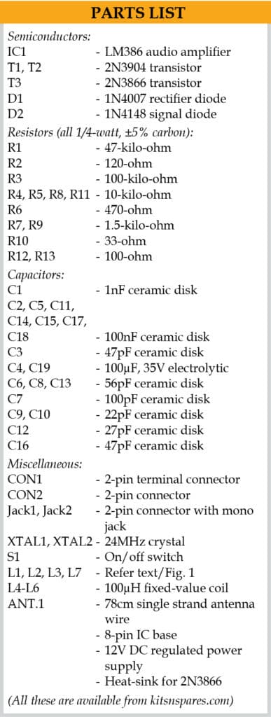
The circuit diagram of the 96MHz crystal-locked simple FM transmitter is shown in Fig. 1. The circuit is built around a low-power audio amplifier using LM386 (IC1), transistors 2N3904 (T1 and T2) and 2N3866 (T3), 24MHz crystals (XTAL1 and XTAL2), rectifier diode IN4007 (D1), signal diode IN4148 (D2) and a few other components.
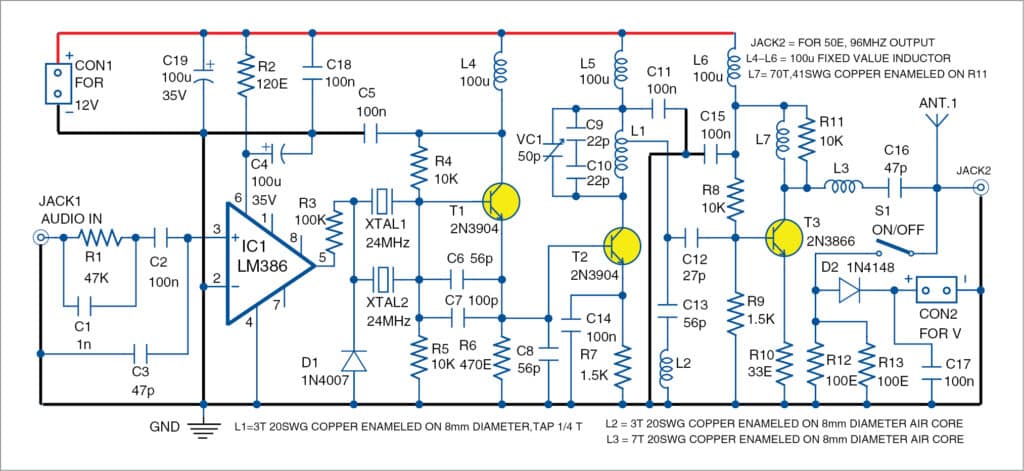
A low-power 24MHz Colpitts oscillator is built around T1 along with biasing resistors R4, R5 and R6, and capacitors C6, C7 and C8.

Transistor T2 is a buffer amplifier and its collector is rich in harmonics. The tank circuit comprising inductor L1, capacitors C9 and C10, and trimmer capacitor VC1 is tuned to four times the oscillator frequency, that is, 96MHz. T2 boosts the fourth harmonic of 96MHz and suppresses the 24MHz fundamental, second (48MHz) and third (72MHz) harmonics by at least -24dBc, or 250 times.
Inductor L2 and capacitor C13 make a series-tuned (72MHz) harmonics trap and attenuate the strong third harmonic to ground. Readymade 100µH moulded inductors (L4 through L6) isolate the power supply from transistors T1 through T3 to help minimise interference between different stages.
T2 feeds power amplifier T3 with approximately 5mW of RF drive via 1/4-turn tap from the top of tuning coil L1. T3 is biased for class A operation. Standing current is set to 20mA with resistors R8, R9 and R10.
40mW of RF power is available at collector of T3. Matching network comprising L3 and C16 transforms output impedance of T3 to 50-ohm impedance of the antenna. (A 78cm long single-strand wire was used as an antenna during testing.)
Audio amplifier IC1’s frequency modulates oscillator T1 by varying capacitance of diode D1, which is connected in series with XTAL1 and XTAL2. (Note that XTAL1 and XTAL2 are connected in parallel to have greater frequency deviation.) The transmitter accepts audio input from an external source such as cellphone. External volume level should be set for best audio level output. R1 and C1 add 50µs pre-emphasis to boost higher audio frequencies. Increasing R1 to 15-kilo-ohm changes pre-emphasis to 75µs.
Construction and testing
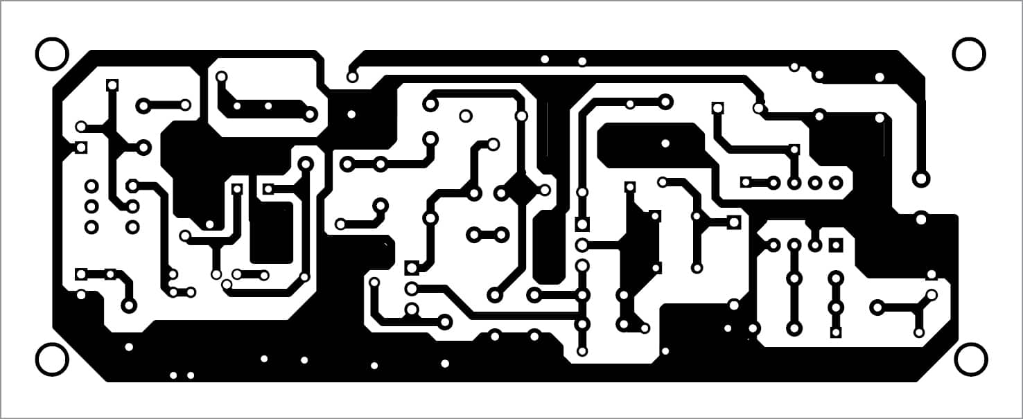
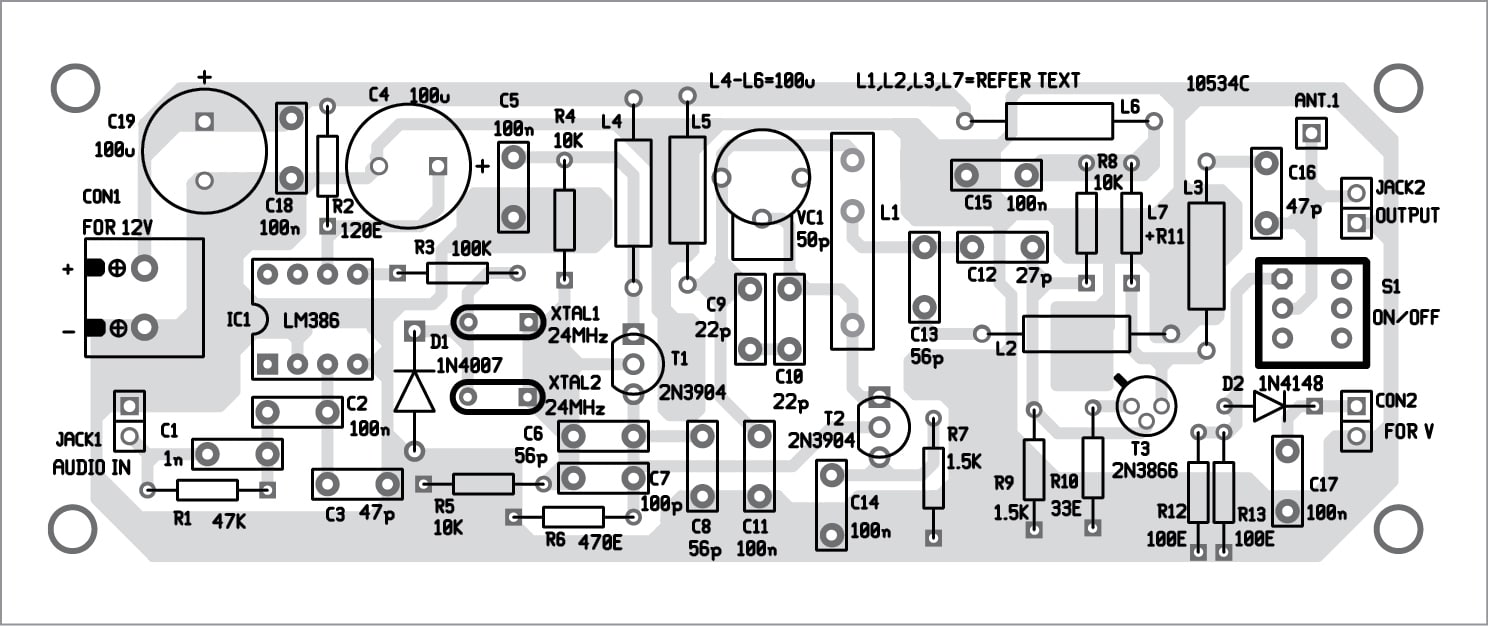
A PCB layout of the FM transmitter is shown in Fig. 3 and its components layout in Fig. 4. After assembling the circuit on the PCB, connect 12V DC across CON1.
Download PCB and Component layout PDFs: click here
Keep all leads short. The prototype was built on a piece of copper-clad board using ugly bug construction method. The large ground plane of the copper board gives excellent results for the VHF circuit. With S1 on and 50-ohm dummy load (R12 and R13) connected, apply 12V regulated power supply.
Carefully tune VC1 for maximum voltage (V) reading at CON2. Output power in milliwatts equals
(V+0.5V diode loss) squared/100
No further adjustment is required.
A cheap USB SDR dongle and free spectrum analyser software may be used to observe output.
Fine tuning of VC1 can also be done using a handheld FM receiver. Make sure a wire antenna is connected in the transmitter circuit.
Now, with FM receiver in your hand, slowly walk away from the transmitter. Correct tuning of VC1 will give maximum range on 96MHz. T3 can be replaced with 2N3904. In this case, increase R10 to 56-ohm. Power output will drop to 15mW.
Use a suitable heat-sink for 2N3866. Care should be taken to keep L1 and L2 2cm apart and at ninety degrees to each other on the PCB.
Spectrum output of the transmitter obtained is in the range of 24MHz to 700MHz. Second and third harmonics of 96MHz are down to -18dBc and -24dBc, respectively. All other spurs or distortions are below -20dBc.
Switch S1 should be off when antenna is connected. Use a shielded cable for input audio connection.
Some inductors are self-made, while others are readymade. L1 is a three-turn 20SWG copper-enameled coil on 8mm diameter air core, tapped 1/4 turns from positive side. L2 also is a three-turn 20SWG copper-enameled wire on 8mm diameter air core. L3 is seven-turn 20SWG copper-enameled wire on 8mm diameter air core. L4 through L6 are 100µH fixed-value coils.
Inductor L7 is made of 70 turns of 41SWG copper enameled wire on resistor R11.
Joy Mukherji is an electronics hobbyist who likes designing radio frequency circuits.
Author here. Many are having trouble finding the 100uH molded chokes used in the circuit. It’s not a critical part at all. It just helps with a cleaner output signal and harmonics are somewhat reduced. Homemade RFC can be made by winding 70 to 100 turns of thin enameled copper wire on a 10K 1/4W or 1/2W carbon film resistor. It can be used in place of 100uH chokes.
The transmit frequency is around 96.045MHz and not 96MHz so an analogue receiver is recommended for receiving the signal.
I made this circuit it’s wonderful and very stable i want to thanks joy for nice project.but I want to increase its volume.mr joy can u help me.when I increase from input it’s distorted.
Use two parallel crystals for slightly increased volume. Since it’s crystal controlled the audio deviation is narrow band and limited. The maximum audio level obtained won’t be as loud as commercial stations. I’ve a different crystal FM transmitter circuit which gives a higher volume. Need the schematic?
Can you share it with me too pls and what for is the cn2?tnx
Hi. Please help me to mske L1. I DO NOT UNDERSTAND what means : L1 is a three-turn 20SWG copper-enameled coil on 8mm diameter air core, tapped 1/4 turns from positive side.
Can u give a photo of coil in this page? Help other please
I used plastic body of a ballpen to wind the coil. Wind 3 turns of 20SWG and then remove the ballpen. You now have an air core coil. The diameter of the ballpen was 8mm.
Tap is at 0.25 or 1/4 turn from V+ side of the coil. Hope this helps.
What is similar to the 2n3866 transistor?
Use 2n3904
Joy Mukherji,
What about a receiver to work with this transmitter?
Google TEA5767 Arduino FM receiver or RDA5708 FM radio with Arduino. I’ve designed a 1W FM band RF amplifier with two PN2222A transistors in parallel? Contact me [email protected] for schematic .
Hello Joy, i need scematic and layout PCB for better volume and the receiver too. Thankyou
It’s NBFM transmiter so TX volume is naturally going to be a little low but you can compensate by increase the volume on receiver side. For receiver, goodle Tea5767 Arduino FM receiver. Google is your friend.
Good day. How do I change the frequency to 100Mhz? Just outside of the commercial range