 Presented here is a low-cost, dual-channel, active AC analog probe. It is suitable for oscilloscopes, multimeters and other analogue measurement equipment.
When experimenting with AM receivers for long, medium and short waves, users need a high-impedance analogue probe with input capacitance below 20pF. The required input impedance from the probe at low frequency is usually one mega-ohm or above.
Most of the low-cost passive probes for oscilloscopes have input capacitance well above 100pF. If you include the input capacitance of the oscilloscope, the total capacitance becomes even higher. The bandwidths of these low-cost passive probes are usually limited to 1-2MHz.
These cannot be connected in parallel with L-C networks in AM receivers because that will change the parameters of these networks significantly.
Circuit and Working
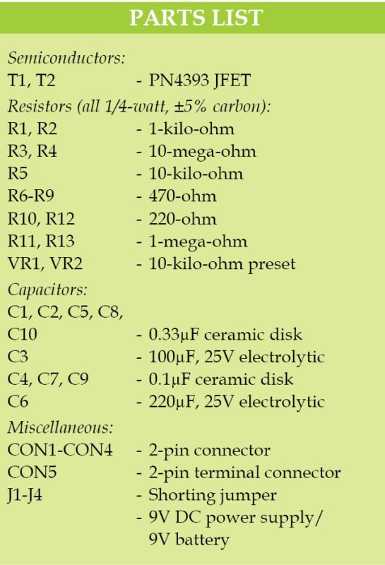
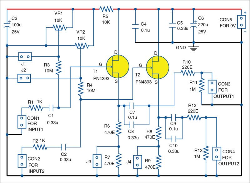
Fig. 1 shows the circuit diagram of the dual-channel, active AC analogue probe. It is built around two n-channel PN4393 JFET transistors (T1 and T2) and a few resistors and capacitors.
Most of the oscilloscopes come with two channels, so you need a dual-channel active probe with common ground and common power supply.
At low frequency, the input resistance of the probe, determined mainly by resistors R3 and R4, is around 10-mega-ohm. At high frequency, the input impedance is determined by the total input capacitance of the probe. With careful implementation and use of appropriate JFETs, you can obtain input capacitance below 20pF.
Transistors T1 and T2 should have low noise level and low input capacitance. So you can choose from transistors like PN4391, PN4392 and PN4393 as these have input capacitance of typically 14pF. You can also use transistors J201, J202, J203, 2N5457, 2N5458 and BF245 (with 1.5dB noise figure). High-frequency JFETs in small cases are preferred but these are costly.
The voltage between the drain and the source of T1 and T2 is adjusted to around half of the power supply, using resistors R6 through R9 and jumpers J3 and J4. The circuitry using resistor R5, presets VR1 and VR2, and capacitor C3 is used to adjust the offset voltage applied to the gates of the JFETs. These components are not mandatory. If you choose not to use these, close jumpers J1 and J2, and connect resistors R3 and R4 to ground.
The gain of each of the channels is slightly below unity, but that is not important in most of the cases. Most oscilloscopes produce a square wave reference signal, which can be used for measurement of the gain and evaluation of the probe.
Construction and Testing
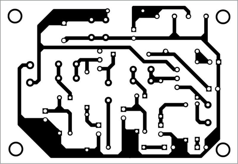
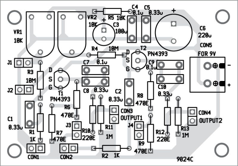
An actual-size PCB layout for dual-channel active AC analogue probe is shown in Fig. 2 and its components layout in Fig. 3. After assembling the circuit on the PCB, enclose it in a suitable cabinet with connectors CON1 and CON2 affixed on the front side and connectors CON3 and CON4 on the rear side of the cabinet.
Download PCB and component layout PDFs: click here
The probe can be implemented on a small PCB. During testing and adjustment, the inputs of the probe can be connected or soldered to L-C networks using very short (3-4cm long) conductors.
Power the circuit using a dry battery or rechargeable battery. The circuit does not require any special adjustment, so you can start using it straightaway after assembly. If you use jumpers J3 and J4, adjust VR1 and VR2 for the best performance of the probe.
After proper implementation, the probe can have bandwidths above 10MHz with a signal generator having low output impedance.