
Knowledge of common pitfalls in electronics circuit design, and how to avoid these, is important for producing any product
While testing a smartphone, the manufacturer finds a major flaw in the device. Some internal body parts have overheated and melted during the stress-test. A root-cause analysis indicates the designed circuit was not optimised for thermal resilience—a step that should have been planned and executed at the start of the design process. There are many such instances where the solution is simple but gets missed amidst the complexity of a design process. That is why designers jot down the list of best practices to ensure they deliver optimal design with minimal rework and resource. In this article, we take a look into some of these best practices and understand their importance.
Common struggles in circuit design
Designers often face issues of rework and wasted resources. This is mainly due to the use of smaller tracks for circuit layout, where all components are not able to fit. Another reason is the rush to meet timelines.
The design team from PCB Power Market, a PCB design and manufacturing firm from India, says, “In a hurry, designers start missing out some essential components. So they start using other objects with simple parts and traces and construct replacements for components. It works initially. The layout looks perfect when they view it. But eventually, they give out.”
Communication with the manufacturer is also critical. If the capacity of the manufacturer is not clear, or if the designer has not shared all the components and design schematic with full clarity, the manufactured end product will be flawed. Along with these come the technical challenges.
The golden rules
Pre-design and post-design analyses are equally important to ensure proper circuit outcome. These involve the following considerations.
Choose the right board spacing
Selecting the right spacing can substantially save cost and rework. According to PCB Power team, “Wherever possible, use wider tracks or spacing. If your design permits bigger tracks via drill size, use them. A via-aspect ratio of 6:1 ensures that your board can be fabricated anywhere. For most designs, a little thought and planning will save cost and improve manufacturability.”
Creating a proper digital representation of the circuit before taking it to production is also important. The PCB Power team continues, “Define all the components and circuit schematic properly in the CAD software during design. In case you have missed out a component, define the component in your CAD library in the correct way and process all the information from there.”
Ensure protection against electrostatic discharge
Electrostatic discharge (ESD) is caused by sudden electrical energy, developed by static electricity or electrostatic induction, flowing from one charged object to another. Electronic circuit components are highly sensitive to ESD. Manufacturing floors and design areas should invest in ESD-protected areas (EPAs) where high-charge objects are kept out.
Ionisation is a popular process for ESD-proofing of electronic devices that cannot be grounded. Use of ESD protector materials during circuit design becomes imperative. Some commonly used ESD protectors include metal-oxide varistors, transient-voltage-suppression diodes, polymer-based ESD suppressors and clamping diodes. ESD protection will keep electronic devices from getting damaged by heavy lightning or any kind of charge transfer.

Save the circuit from EMI
Electromagnetic compatibility (EMC) is crucial to ensure the quality of the circuit being designed. It ensures that electronic circuits are not troubled by electromagnetic interference (EMI).
EMI arises due to radio-emission of other nearby electronic objects. It impacts electronic circuits by providing wrong data or making the system stop altogether. EMI shielding can be done by using components like ferrite beads and capacitor filters. Overall, EMC can be controlled using shielded inductors to cut down sharp current transients. There are also EMI shielding materials that can keep the PCB unaffected.
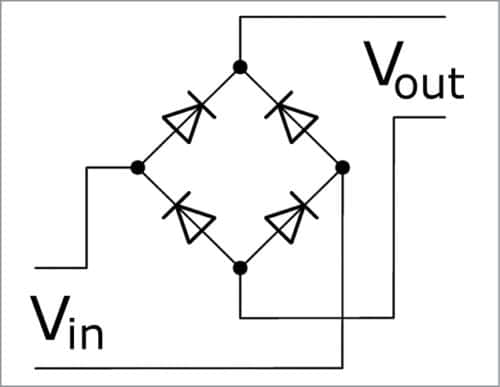
Create resilience to reverse polarity
There is always the chance that the two charged ends of an electronic device get connected to the wrong terminals. One of the most common examples is attaching a battery in reverse polarity to an electronic device. If the circuit design is not well-protected against reverse polarity, hazardous outcomes might follow, including malfunction or even frying of the circuit. One precautionary measure is to connect the heavy-load-carrying microprocessor output drivers to a large resistor. Using a diode bridge is another option that rectifies the input and ensures correct polarity in the circuit.
Tend to each component separately for thermal resilience
Electronic circuits can lead to disasters if their components are not tested for heat resistivity.
The process to ensure thermal stability at peak temperature differs for every component. For instance, a resistor’s capacity is determined by measuring the de-rating of power at peak temperature. Capacitance, on the other hand, can be checked by evaluating the leakage rate, increase in equivalent series resistance capacity and de-rating. For diodes and transistors, current gain and recovery time under peak temperature can be essential determinants.
Evaluate the circuit behaviour with power
It is essential to know the behaviour of the circuit when it is connected to a power source. Measuring the pull-up resistors can help you know whether the circuit is behaving properly during power-up. Pull-up resistance on a logic circuit’s microcontroller units should be high on power-up.
You should also know how your circuit design will function if there is a sudden outage in power while it is processing some data. Including a power-down detection circuit is very important to ensure that the processor is saving the information properly during a sudden power cut. Power-off detection circuit is a network of a diode and a collection of capacitors, transistors and a voltage-generating circuit that keeps a circuit running for some time with its discharged power during power-cut.
Also, take precautionary measures for current overshoots and undershoots in the circuit. These are basically spikes and falls in the current flowing through a circuit. Very high overshoots may fry the circuit. On the other hand, excessive falls can hamper the circuit functioning. Use of clamping diodes is a good option to ensure the safety of circuit terminals from such power inconsistencies.
Test points are important
Test points are small wired loops placed on a PCB board to allow easy anchoring of test probes on the circuit. Usually, test probes are made of phosphor-bronze alloy with copper conductors or silver-plate coatings. Ground nets, power nets and threshold points of circuits should be mandatorily assigned test points.
Be clear with your manufacturer
As mentioned before, clarity with the manufacturer right from the start is very essential. To avoid complications, learn about the manufacturer’s specifications including minimum trace width, spacing and number of layers. You must have complete transparency while sharing the design details. Mention all the components, the schematic and the build. In case a custom-built circuit is desired but has not been communicated to the manufacturer, they would be following the default build model, which might create great differences from the expected outcome.
Electronic circuit design is not easy
Nevertheless, if done well, it can do wonders—whether you are doing a small-scale project or a large-scale business. Thus, keeping the rulebook open will keep you a step ahead in the game.