Despite its critical nature in high-speed circuitry, PCB layout is often one of the last steps in the design process. This article aims to help designers be aware of the various considerations they need to address when designing board layouts for high-speed circuitry.

Better the designing, better the PCB manufacturing! PCB layout is an important step in the designing of any electronic device. It determines the success or failure of a piece of equipment. With the constant evolution of technology, complexity and expectations of PCB designs have reached new heights. Thus, PCB design rules and production processes have also evolved to achieve new layouts and capabilities.
PCB design software has helped with this progression by providing tools that help electronics engineers to design better PCBs from the ground up. A PCB is essential for everyday appliances and industrial machines alike. PCB technology will need to adapt to the fast-paced world to allow the devices to keep up with the growing demand for speed.
Current and future trends in high-speed design
New software tools and methods are constantly under development to manage high-speed designs. Between wearable electronics, flexible displays and medical applications, flexible technology is the fastest growing segment of the PCB industry. Due to their flexibility, flexible and flex-rigid PCBs can handle more stress and bending than rigid PCBs. These can even be folded to fit into 3D spaces. These are light, thin and yet relatively easy to manufacture in mass quantities.
e-Scrapping continues to be a problem as people try to find ways to get rid of old electronics. There are many organisations working to curb this problem by picking waste from desired locations for recycling of the same. The idea of extracting precious metals from e-waste to reuse them is great. This could reduce the pressures on mining companies to produce vast amounts of metal for the electronics industry. Biodegradable substrates are a good alternative, which is currently under close examination. Both of these methods could help reduce the impact of the electronics industry on the environment.
In the mobile telecom industry, interconnect and board dimensions are reducing in size rapidly. Nowadays, PCBs are utilising fewer but more complex components. Boards for networking and computer applications require more interconnect and plane layers. Understanding which tools will best support the needs of design is therefore necessary.
Electronics companies require best PCB design tools with effective libraries, infrastructure, design data and designers. These allow design teams working at different locations to work on the same project at a time.
Latest technology for PCB fabrication, design and interconnects
One of the upcoming trends is using PCBs as active system components. Currently, PCBs are used as connecting components in electronics, relaying messages between active components so the complete device can work. Engineers are currently working on active PCBs, which will reduce the number of components in the PCBs while maintaining functionality.
Augmented reality (AR) and virtual reality (VR) could change the face of electronics design, as these are making rapid inroads in the consumer electronics world. Their potential application in PCB design is to address issues such as fitting electronic packages into unconventional shapes. This will ensure circuit connections work properly and reduce the time-consuming process of place-and-route.
The idea of training using AR with simulation software is also under exploration. In the near future, augmented PCBs could be used to reduce cost and wastage of materials used in current training methods. It could replicate magnetic and electric fields generated by a product as an alternative way to ensure that the product meets regulations. “Much like the integration of 3D into PCB design, AR is a solution to many problems of advanced technology,” says Ben Jordan, senior manager product and persona marketing, Altium.
As consumer demands change, so must technology. High-density interconnect (HDI) boards are one of the fastest growing technologies. These have higher density circuitry than traditional circuit boards. This provides designers the option to place more components on both sides of the PCB.
Multiple via processes allow designers to place components that are smaller even closer together. Decreased component size allows more input/output in smaller geometries. This results in faster transmission of signals and significant reduction in signal loss.
A PCB board camera is mounted directly onto a circuit board. It consists of a lens, aperture and image sensor. It is designed to take both digital pictures and videos, and can be mounted on any PCB, irrespective of size.
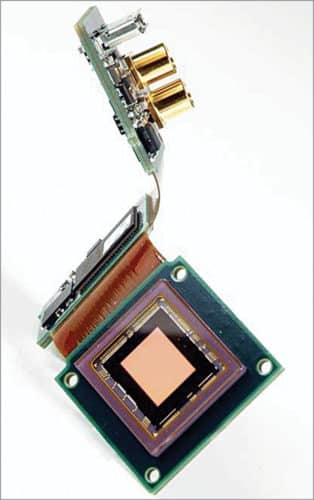
Board cameras have developed quickly to take high-resolution images and videos with ease. In the future, board cameras are expected to develop to create powerful solutions for both industry and consumer electronics.
Small board cameras have found important applications in the medical industry for non-invasive and minimally-invasive procedures. Pill-sized cameras allow doctors to take comprehensive videos and images from inside the digestive tract without invasive surgery. These small cameras can also be used to monitor homes and businesses for intruders.
3D polyethylene (PE) manufacturing is expanding the types of materials that can be used for circuits. It makes use of flexible and biodegradable substrate materials more feasible.
Combinations of these innovative ideas will enable PCB designers to accomplish incredible new designs that will keep the industry moving forward. Thus, PCB technology will continue to advance into the future as needs and priorities change.
3D PE manufacturing techniques enable circuits to take new shapes to fit in any circuit carrier, while still combining electronic, optic and mechanical functions. These include developing different types of surfaces for printing, surface-mount devices and manufacturing tools that can be used to print these. Many industry leaders expect the 3D PE industry to expand quickly with new methods and applications for 3D PE technology. This will help improve product features and optimisations. Increased automation reduces the likelihood of failure by human error and improves overall efficiency. These benefits have led to rapid 3D PE production advancements.
Signal integrity is an integral and essential part of the PCB design process. With increase in demand for high-speed circuits, it is not possible to design the basic circuit in isolation from just the PCB design. Instead, it must be a part of the overall electrical design. This approach can minimise the possibility of problems arising from poor signal integrity.
A high-speed PCB is one where integrity of the signal is affected by the circuit layout. In digital PCB signal, effects on signal integrity can manifest as delayed or cancelled digital signals. In a high-speed analogue circuit, signal integrity problems appear as altered signal shapes.
Challenges and development areas in PCB designing
Poor electromagnetic compatibility (EMC) is one of the main reasons for PCB re-designs. This is most likely because there are stringent regulations in sectors such as medical and aerospace that require EMC value to be under control throughout use. So, products being developed are designed with this in mind.
For instance, cellphone developers require wireless connectivity and are well-versed in minimising the risk of unwanted radiations. The most affected equipment of EMC issues are toasters, fridges and washing machines. These are joining the plethora of Internet-enabled devices connected wirelessly to the Internet of Things (IoT). Potentially high-volume boards may result in re-spinning PCBs, which can introduce further product launch delays.
Built-in electrostatic discharge (ESD) protection systems are required for circuit design and component selection. One should always make sure to leave enough time for PCB layout. Since today’s boards are becoming more complex, compact and lightweight, designing requires close observation and advanced instruments.
Growing popularity of flexible PCBs complicates the process further. An inadequate layout can result in problems such as electromagnetic interference (EMI), conflicts from components on either side of the board, limited board functionality and even total board failure. If designers do not get the layout right the first time, they will need to rework it, which can cause manufacturing delays and added costs.
To sum up
Information about current and future trends in high-speed design is endless, but it is essential to be updated with recent trends, including FPGA-on-board integration, team design, and library, constraint and data management. This will help to address challenges and solutions associated with each area and the underlying PCB design industry.