
This article covers some important issues in design of high-frequency electronic circuits and commonly followed practices to mitigate them.
Electronic circuits behave very differently at high frequencies. This is mainly due to a change in the behaviour of passive components (resistors, inductors and capacitors) and parasitic effects on active components, PCB tracks and grounding patterns at high frequencies. The change of behaviour also causes electromagnetic interference (EMI) problems. This article discusses these effects and some commonly followed practices to mitigate them.

Ideal components
Resistor
In time domain, the instantaneous voltage and current for an ideal resistor are related by:
v=iR ——-(1)

where R is the resistance and v the energy lost per unit charge when it flows from positive terminal to negative terminal. The energy lost is converted into heat by the resistor.
In frequency domain, phasors for sinusoidal voltages and currents are related by:
V=IR ———-(2)
Thus the voltage-current relationship is independent of frequency.
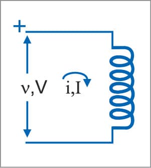
Inductor (energy storage element)
In time domain, voltage-current relationship for an ideal inductor is:
v=Ldi/dt ———(3)
where L is the inductance and t the time.
Since v is the energy lost per unit charge, when charge flows from the positive terminal to the negative terminal, this energy is used for increasing current as per the above equation. The magnetic field inside the inductor coil is proportional to the current. Hence the energy is used in building up the magnetic field and stored in the magnetic field.
In frequency domain, phasors for sinusoidal voltages and currents are related by:
V=j(Lω)×I ——–(4)
where L is the inductance in Henry, ω the angular frequency of driving sinusoid voltage source in radians/second and j=√–1
Hence the voltage-current relationship for inductors varies with frequency.
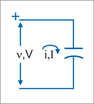
Capacitor (energy storage element)
In time domain, voltage and current for an ideal capacitor are related as:
![]()
where q is the charge accumulated on the capacitor at time t, c the capacitance and t the time.
The charge accumulated on the capacitor establishes an electric field between plates of the capacitor and thus the capacitor stores energy in the form of electric field.
In frequency domain, phasors for sinusoidal voltages and currents are related by:
![]()
where C is the capacitance in Farad, the angular frequency of driving sinusoid voltage source in radians/second and j=√–1
Hence, the voltage-current relationship for capacitor varies with frequency.
Behaviour of components at high frequencies
Wires
At high frequencies, wires behave as inductors (opposing changes in the current) besides their natural low resistance value.
Resistors
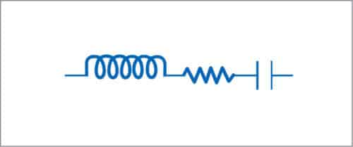
At high frequencies, resistors behave as series inductors (opposing changes in the current) and parallel capacitors (opposing changes in the voltage) besides their natural resistance.
Inductors
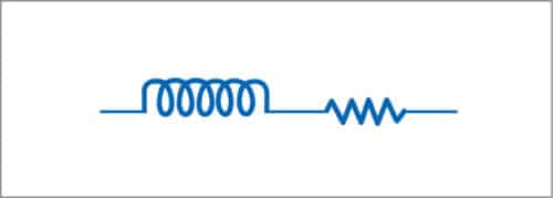
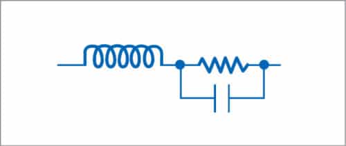
At high frequencies, inductors behave as series resistors and parallel capacitors besides their natural inductance.
Capacitors
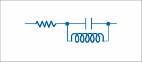
At high frequencies, capacitors behave as series resistors and series inductors besides their natural capacitance.
Thus, simple voltage/current relationships for ideal components are no longer valid at high frequencies and suitable circuit analysis methods are to be used by replacing them with their high-frequency equivalent circuits.
PCB tracks
PCB tracks behave like wires at low frequencies. This behaviour is no longer sustained at high frequencies. To understand this behaviour, you have to understand how a signal is transmitted from a source to the receiver and transmission line theory. Fig. 8 shows a source/driver delivering signal to a load/receiver through wires (shown by lines).
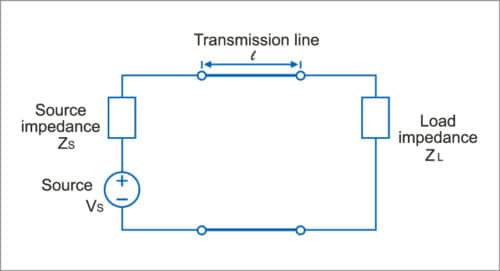
At low frequencies, connecting wires from the transmitter/source to the receiver/load have very low resistance and act as short-circuit. Voltage from the source is directly applied to the receiver. Any change in voltage at the source is delivered instantaneously at the same time to the receiver. Appropriate current flows from the positive lead of the source through connecting wire and the load and the return wire, to the negative terminal of the source.
The value of current depends on the source voltage and the load.
Normally, source and receivers are components soldered on PCBs and connecting wires are tracks on PCBs. Send and return PCB tracks behave like a transmission line if the signal frequency of the source is sufficiently high.
Lumped transmission line model represents send and return lines to have resistance (R), inductance (L), capacitance (C) and conductance (G) per unit length. Their values depend on spacing between send and return lines, thickness of lines, transmission medium, etc. Since these lines are copper tracks on PCBs, their values are dependent on PCB tracks’ thickness and separation, that is, PCB tracks’ geometry and board material. These parameters cause voltages and currents to travel like waves through transmission lines (PCB tracks).Any change in voltage/current at the source is transmitted like a wave and reaches the receiver after wave propagation delay. This delay is dependent on transmission line parameters, that is, PCB tracks geometry and board material. At low frequencies of source signal, this delay is much smaller than rise/fall time of the signal. At sufficient high clock/signal edge rates, delay becomes comparable to the rise/fall time of the source signal/clock.
Transmission lines have an important characteristic called characteristic impedance (Z0), which depends on R, L, G, C and thus PCB tracks geometry and board material. Equations derived in transmission line theory using lumped parameter model show that at any instant of time, and at any point on transmission line, voltage/current values are obtained as the sum of a forward travelling wave from the source to the load and a reverse travelling wave from the load to the source. The reverse travelling wave is called reflected wave from the load.
If load impedance exactly equals Z0, amplitude of the reflected wave will be zero and there will be no reflected wave from the load. In this case, signals from the source are transmitted to the load without any distortion.
If load impedance does not equal Z0, there will be a reflected wave from the load to the source. This situation is called impedance mismatch. If there exists impedance mismatch at source side also, the reflected wave will be reflected back again from the source to the load. Thus there will be multiple reflections on both sides. Transmission line also attenuates the amplitude of forward and reflected waves along its length. Hence the amplitude of each successive reflected wave is reduced. These impedance mismatches and reflections cause the signal sent from the source to be distorted at the load end, giving rise to a phenomenon called ringing. This can be avoided by following appropriate resistor termination practices at the load side and/or the source side.
The rule of thumb for considering PCB tracks from a source to the load as transmission line is that the total propagation delay of the signal should be greater than one-sixth the rise/fall time of source pulses. This phenomenon is called signal integrity (SI). Software tools can be used to assess and fix proper values of terminating resistors and preserve signal integrity at the load end.
Electromagnetic interference
In the simple circuit of a source/driver delivering a signal to the receiver in Fig. 8, let us assume that the rise/fall time is such that wires need not be treated as a transmission line. Even in this case, if the frequency of current in the loop is sufficiently high, electromagnetic radiation from the current loop will give rise to disturbance in the operation of nearby electronic circuits. The current loop will also get affected by electromagnetic radiation from nearby circuits. This phenomenon is called electromagnetic interference. The EMI generated, or susceptibility to the EMI, is proportional to the frequency of current in the loop and loop area. Hence loop area needs to be minimised to minimise EMI.
As the source and receivers are components soldered on PCBs, and connecting wires are tracks on PCBs, care is to be taken during layout stage that send and return traces are nearby in single-/two-layer PCBs. If send and return traces are far away, it will result in larger current loop area, causing EMI problems at sufficiently high frequencies. In many cases, the return trace is nothing but signal ground. In a single-/double-layer PCB, every signal line should have ground trace just by its side—it is better to have the signal trace surrounded by ground traces on either sides.
If a PCB is very dense and doesn’t have space for so many signals and ground traces, multilayer PCB is a better solution. Alternate layers can be used for signal, ground and power planes—for example, layer 1 as signal plane, layer 2 as ground plane, layer 3 as power plane and layer 4 as another signal plane.
Here is how this concept works: High-frequency current always tries to follow a path that minimises the occupied current loop area because that path only provides minimum inductance/impedance. All signal traces in the signal plane can use any path below the ground plane for return current. This results in minimum loop area for all signal traces and thus minimum EMI/susceptibility. Signal traces in layer 4 use layer-3 power plane for high-frequency AC return currents. Many grounding and layer stacking schemes are available in literature to take care of these aspects.
Crosstalk
If two signal tracks run very close to each other on a PCB, there will be capacitive coupling between them. High-frequency signal changes on one signal will get transmitted to the other signal because of capacitance. This phenomenon is called crosstalk.
Minimum separation between signal tracks is required to avoid crosstalk. Signal tracks in consecutive layers of a double-sided PCB should be run perpendicularly to avoid crosstalk.
Power supply decoupling
In Fig. 8, assume that the load is the switching load of a digital IC, the source is the power source for that IC and lines shown as transmission line are power supply rails for the IC containing switching load. Normally, the actual power source will be in another power supply card of the unit and voltages will be delivered through connector pins of the card to which this digital IC belongs. Voltages will be delivered to connector pins of the card either through wiring or through a motherboard. Power supply lines from connector pins to the digital IC will run through PCB power tracks. This total current loop will have some inductance because of lengthy power lines and the enclosed large loop area if care is not taken in the PCB layout.
Digital ICs source/receive large switching currents when logic gate circuits containing transistors switch states from high to low or vice versa. If rise/fall time is very low, this switching of current takes place in a very short time. This large change of switching current in a short time results in a voltage drop as per Eq. (3) and voltage spikes appear between actual power pins of the digital IC. If the total current loop area is large, this can result in EMI also.
Solution to this problem lies in putting power-supply decoupling capacitors between power and ground, one for every digital IC, and at the connector pins where power enters the board. These capacitors will provide the required switching current, without drop in voltage, from their stored charge acquired from power rails. They will regain through power rails the charge lost in supplying the switching current after switching is over. Decoupling capacitors also reduce the effective loop area of switching current since it is supplied by the nearest IC decoupling capacitor. Thus these reduce EMI also.
Usually, 0.1µF ceramic capacitors are used for digital ICs. 10-100µF tantalum capacitors in parallel with 0.1µF ceramic capacitors are used at connector pins where power enters the board. Tantalum capacitors exhibit more inductance at frequencies greater than a certain value, because of which ceramic capacitors are used in parallel to cover a higher frequency range. Simulation tools are available to fix location and values of decoupling capacitors, which need to be used for accurate design.
Knee frequency
If you observe the spectrum of a digital signal on a spectrum analyser, you will find that most of the energy is contained in the frequency band up to a frequency called Knee frequency. The energy rolls off at the rate of -20dB/decade up to knee frequency. Beyond knee frequency, it rolls off much faster. Hence it is considered that most of the energy of a digital signal is contained in the frequency band from 0 to knee frequency, represented as Fknee. Value of Fknee is related to rise/fall time of digital edges, but not to clock rate.
Fknee is given by:
Fknee = 0.5/Tr
where Tr is the pulse rise time/fall time, whichever is lower.
Hence all digital circuits should have a flat frequency response up to Fknee to pass digital signal without distortion.