


FPGAs and ASICs are widely used nowadays, especially in electronics equipment such as laptops, smartphones, and television sets. The components have their strengths and weaknesses. Their suitability depends on the type of application. With time, it is hoped that FPGAs and ASICs will undergo new advancements and efficiently meet customer needs.
FPGAs and ASICs form the core of modern-day electronics systems. Without them much of the equipment that we take for granted would cease to exist. But there is more to what meets the eye. Behind the state-of-the-art processors, months and years of effort makes them robust and reliable. So let us find out more about their design journey.
Application specific integrated circuit, or ASIC, is a type of IC that is used only for specific applications. Field programmable gate array, or FPGA, is an IC that can be repeatedly used for different applications as it is reprogrammable. To do so, one needs to rewrite the Hardware Design Language (HDL) code and reprogram the FPGA accordingly.
Some other differences between them are:
Time to market
ASIC is notoriously slow when it comes to time to market. A good ASIC may take five to six years to get fully developed from scratch. On the other hand, FPGA projects such as PCI and USB require eight months to a year to get ready.
Unit cost
The per-unit cost of FPGA is high as compared to ASIC. For that reason, FPGAs get developed only when a large number needs to be produced.
Power consumption
Nowadays, power consumption is a big issue. We want our electronic devices to save battery power and work efficiently, even on low power. From this perspective, FPGA is not a good choice since it has high power consumption rate compared to ASIC.
Frequency
FPGA operates at a much less frequency as compared to an ASIC. The operational difficulty increases at higher frequencies. For an ASIC, however, there is no specific frequency speed.
Design complexity
An ASIC is complicated to design and manufacture, therefore it takes a long time to market. But FPGA is comparatively simpler.
FPGA design flow
The process of designing an FPGA generally begins with functional specifications at the top. Next, the HDL code is written on which behavioural simulation is performed. After that come the steps of synthesis, place & route, download and verify, along with static timing analysis, which are handled by the designing software.
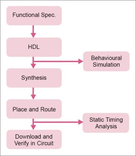
For a Xilinx FPGA, the Vivado software is used. For an Intel FPGA, Quartus is used. In Vivado, the step Place & Route is also known as Implementation.
During behavioural simulation, the HDL code is checked for its accuracy and expected behaviour, that is, whether the code has any functional bug in it or not.
During static timing analysis, the setup time and hold time violations are checked. Although hold time delay can be a bit difficult to resolve, setup time is easy if you have a good understanding of the design functionality.
Finally, a bitstream is generated, which has to be downloaded and designed into the FPGA for circuit verification.
ASIC design flow
The design process of ASIC also begins with functional specifications, which move onto the HDL code. Behavioural simulation is done using Questa sim, Model sim, and such other simulators. Before proceeding to synthesis, there is a step called DFT Insertion where flip-flop connections are checked for any faults. After synthesis, the static time analysis (STA) needs to be performed for which a specific STA engine is required. Therefore, the setup time and hold time delay need to be removed. However, their removal is quite challenging since they work at a very high frequency. (ASICs generally work at a very high frequency as compared to FPGAs.)
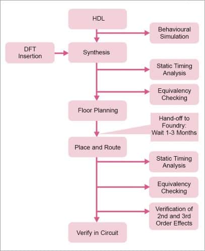
Next is equivalency checking and floor planning, which is related to standard cell libraries in an ASIC. Here, the HDL is converted into RTL. Floor planning is the step where the standard cell is replaced from the logical library onto the chip.
After that the design is given to the foundry. But before doing so it must be ensured that there are no mistakes or bugs in the design, else that will result in a huge loss. Initially, the foundry produces about 100 chips for basic testing. If a bug is found in the testing process, the entire process has to be repeated from the synthesis and floor planning stage until all the bugs have been removed from the ASIC. This takes a lot of time and, as a result, the time to market increases. This is the reason why FPGA is preferred for design prototyping.
After a wait of one to three months for the bug-free ASIC chips to arrive from the foundry, the next step is of place & route where STA is again performed to make wire connections (related to input-output).
Then comes the verification of second and third order effects. Once the faults have been rectified, the circuit needs to be verified. This is done by putting the ASIC on the board along with the other components. After confirmation that the ASIC’s operation meets expectations, it is released into the market.
So, ASIC has a lengthy design flow and takes a lot of time to manufacture, whereas FPGA takes much lesser time.
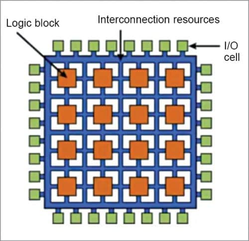
FPGA structure and its accelerated flow
Fig. 3 shows the inside on an FPGA, where the green coloured boxes are known as I/O Cells. The orange coloured boxes, called Logic Blocks, consist of configurable logic blocks (CLBs) and look up tables (LUTs). Depending on the FPGA, the I/O cells and the logic blocks can change. The blue coloured lines represent the programmable interconnect resources, which allow the generation of different bit files.
If a bug is detected while verifying an FPGA circuit, a change is made in the HDL code to correct it, while the behavioural simulation is checked for any broken flow. Then the bit file is generated and later tested on the board to check its working. Generally, 3-4 days are required to correct a bug in FPGAs. But in ASICs that increases up to 6-7 months.
Once the ASIC RTL is designed, it is prototyped onto an FPGA to verify the design functionality. The benefit is that, with the help of RTL, bugs can be resolved easily along with any CDC or STA violations. However, it must be noted that there is no guarantee that the code result will be 100% bug-free. Only 60-80% of bugs can be resolved in the FPGA. The rest 40-20% of bugs have to be resolved in ASIC only.
FPGA can only accelerate the detection of bugs, which would take a lot of time to get resolved in ASIC. After detecting the bugs, the RTL is again changed from an FPGA to ASIC.
Peripheral connections
From Fig. 4 we can see that the chipset, CPU, and various other peripherals are externally connected to an FPGA because FPGA does not provide the facility to embed the CPU within itself (although many companies like Xilinx are working on changing that). This scenario, however, is absent in an ASIC, where the CPU can be embedded directly inside the ASIC.

Design challenges of ASIC
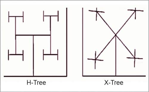
One of the major challenges faced in designing ASIC is clock routing (CLKrouting). In ASIC, the clock should be routed properly so that it reaches every flip-flop at the same time to prevent clock skew. For that purpose, there are H-tree and X-tree types of circuit. In H-tree as well as X-tree, the clock is given at the intersection (of the letter H or X) as shown in Fig. 5. The flip-flops are placed on the edges, allowing the clock to reach simultaneously without any clock skew.
Next come power routing and ground (GND) routing. In ASIC, there are different layers for power and ground channels, which are connected using a via. The drilling of a via connection gives different chip layers for power routing and ground routing.
The next challenge is crosstalk. If the distance between two parallel signal lanes is too small, the signals may interfere with each other. Therefore, a specific distance must be maintained. Then we can download the bitstream into the FPGA and run it. The issue of crosstalk exists in ASIC but not in FPGA.
Since there are no flip-flop problems in an FPGA, its utilisation is quite high. But an ASIC should not heat up and should work in both low and high temperatures. If the flip-flops are placed too close to each other, two different parts of the ASIC may have different temperatures, thus creating a design failure. So, we have to ensure that the circuit routing is done perfectly. We do not have to worry about this problem in FPGAs since the Vivado software places them in small parts at different blocks of the FPGA.
Design challenges of FPGA
An ASIC is first tested in an FPGA before being launched. But one of the major drawbacks in this prototyping method is that the FPGA runs at a low speed as compared to an ASIC. ASIC runs at a fast clocking speed, which cannot be matched by an FPGA.
The next drawback is the power consumption. ASIC can operate on very low power as compared to an FPGA.
Also, latches cannot be accommodated in the FPGA since everything is present in the form of flip-flops and LUTs. But latches can be easily implemented in ASICs.
Other prototyping methods
Emulators can be used as a prototyping method and help in reducing the time to market even further than FPGAs. However, these are expensive and were launched just a few years ago in the market. FPGAs have been there for many years.
For thousands of signals and hundreds of lines of HDL code, emulators provide a full signal debug for our design, allowing us to precisely locate a bug in a particular part of the code.
One of the emulators is the Veloce emulator provided by Mentor Graphics for prototyping an ASIC.
The article is based on the talk ‘Rapid Prototyping Solutions: The Role Of FPGAs’ by Abhinav Behl, RTL Designer at LogicFruit Technologies, which was presented at February edition of the Tech World Congress 2021.
