


Flip-flops in digital electronics are circuits with two stable states that can be used to store binary data. The stored data can be changed by applying varying inputs. Flip-flops and latches are fundamental building blocks of digital electronics systems used in computers, communications, and many other types of systems. Both are used as data storage elements.
Table of Contents
Why is it called Flip Flop?
Its name comes from its ability to “flip” or “flop” between two stable states. By latching a value and changing it when triggered by a clock signal, flip-flops can store data over time. They are called flip-flops because they have two stable states and switch between them based on a triggering event.
It is the basic storage element in sequential logic. But first, let’s clarify the difference between a latch and flip-flops in electronics.
Flip-Flop v/s Latch
The primary difference between a latch and a flip-flop is the gating or clocking mechanism.
In Simple words, flip-flops are edge-triggered, and latches are level-triggered.
If you are confused between latch and flip-flop, then you should check this detailed article where we discussed the difference between Latch and flip-flop.
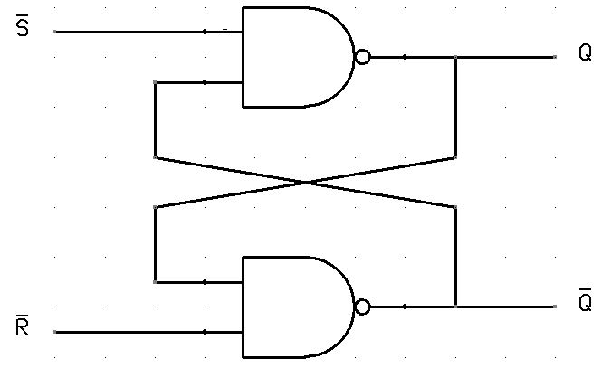
For example, let us talk about SR latch and SR flip-flops. In this circuit, when you Set S as active, the output Q will be high and Q’ will be Low.
This is irrespective of anything else. (This is an active-low circuit; so active here means low, but for an active high circuit, active would mean high)
A flip-flop, on the other hand, is a synchronous Circuit and is also known as a gated or clocked SR latch.
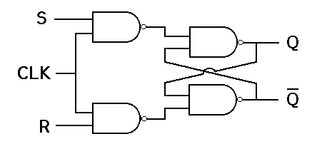
In this circuit diagram, the output is changed (i.e. the stored data is changed) only when you give an active clock signal. Otherwise, even if the S or R is active, the data will not change.
What Device is a Flip-flop? A flip-flop is not a specific device but rather a term used to describe a group of sequential logic circuits. These circuits made up of digital logic gates and other components, can be created using different electronic elements like transistors, integrated circuits (ICs), or programmable logic devices (PLDs).
Let’s understand the flip-flop in detail with the truth table and circuits.
Types of Flip-flops with Truth Table
There are 4 types of flip-flops in digital electronics:
- SR Flip Flop
- JK Flip Flop
- D Flip Flop
- T Flip Flop
Let’s understand each Flip-flop one by one.
1. SR Flip Flop
This is the most common flip-flop among all. This simple flip-flop circuit has a set input (S) and a reset input (R). In this system, when you Set “S” as active, the output “Q” would be high, and “Q‘” would be low.
Once the outputs are established, the wiring of the circuit is maintained until “S” or “R” goes high, or power is turned off.
As shown above, it is the simplest and easiest to understand. The two outputs, as shown above, are the inverse of each other.
SR Flip Flop is also known as a master-slave flip-flop.
The truth table of SR Flip-Flop is given below.
| S | R | Q | Q’ |
| 0 | 0 | 0 | 1 |
| 0 | 1 | 0 | 1 |
| 1 | 0 | 1 | 0 |
| 1 | 1 | ∞ | ∞ |
Check the detailed explanation of SR Flip Flop.
2. JK Flip-Flop
Due to the undefined state in the SR flip-flops, another flip-flop is required in electronics.
The JK flip-flop is an improvement on the SR flip-flop where S=R=1 is not a problem.
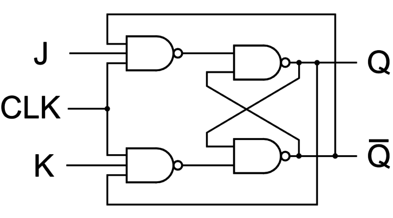
The input condition of J=K=1 gives an output that inverts the output state. However, the outputs are the same when one tests the circuit practically.
In simple words, if J and K data inputs are different (i.e. high and low), then the output Q takes the value of J at the next clock edge. If J and K are both low, then no change occurs.
If J and K are both high at the clock edge, then the output will toggle from one state to the other. JK Flip-Flops can function as Set or Reset Flip-flops.
JK Flip-flop Truth Table:
| J | K | Q | Q’ |
| 0 | 0 | 0 | 0 |
| 0 | 1 | 0 | 0 |
| 1 | 0 | 0 | 1 |
| 1 | 1 | 0 | 1 |
| 0 | 0 | 1 | 1 |
| 0 | 1 | 1 | 0 |
| 1 | 0 | 1 | 1 |
| 1 | 1 | 1 | 0 |
Check the detailed explanation of the JK Flip Flop.
3. D Flip-Flop
A delay or D flip-flop is a better alternative that is very popular in digital electronics. They are commonly used for counters, shift registers, and input synchronization.
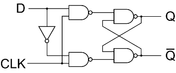
In the D flip-flops, the output can only be changed at the clock edge, and if the input changes at other times, the output will be unaffected.
Truth Table:
| Clock | D | Q | Q’ |
| ↓ » 0 | 0 | 0 | 1 |
| ↑ » 1 | 0 | 0 | 1 |
| ↓ » 0 | 1 | 0 | 1 |
| ↑ » 1 | 1 | 1 | 0 |
The change of state of the output is dependent on the rising edge of the clock. The output (Q) is the same as the input and can only change at the rising edge of the clock.
Check the detailed explanation of the D Flip Flop.
4. T Flip-Flop
A T flip-flop is like a JK flip-flop. These are single-input versions of JK flip-flops. This modified form of the JK is obtained by connecting inputs J and K together. It has only one input along with the clock input.
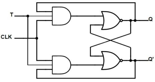
These flip-flops are called T flip-flops because of their ability to complement their state, i.e. Toggle, hence they are named Toggle flip-flops.
Truth Table:
| T | Q | Q (t+1) |
| 0 | 0 | 0 |
| 1 | 0 | 1 |
| 0 | 1 | 1 |
| 1 | 1 | 0 |
Check the detailed explanation of T Flip Flop.
Applications
There are various types of flip-flops being used in digital electronic circuits, and the applications of Flip-flops are as specified below.
- Counters
- Frequency Dividers
- Shift Registers
- Storage Registers
What’s the Major Role of Flip-flops in Computer Electronics? Flip-flops play a critical role in computer electronics by serving as memory elements, storing state information, ensuring clock synchronisation, enabling digital counting, and facilitating control logic. They are essential for data storage, sequencing, coordination, and control within a computer system.
Flip Flop Conversion
Flip-flop conversion refers to the process of modifying one type of flip-flop (e.g., SR, D, JK, or T) to behave like another type by designing an appropriate input logic circuit. This is often required when a specific flip-flop is not directly available or for simplifying circuit design.
General Steps for Flip-Flop Conversion
- Understand the Source and Target Flip-Flops:
- Identify the type of flip-flop you have (source flip-flop) and the type you want to convert it into (target flip-flop).
- Know the characteristic equations and truth tables for both types.
- Write the Truth Table for the Target Flip-Flop:
- Create a truth table for the target flip-flop based on its characteristic equation and behaviour. Include the current state (Q), the input of the target flip-flop, and the next state (Qnext).
- Relate the Target and Source Flip-Flops:
- For each possible combination of Q (current state) and Qnext (desired next state), determine the required inputs for the source flip-flop to achieve the same behaviour.
- Determine the Input Expressions:
- Derive the logic expressions for the inputs of the source flip-flop that will allow it to produce the same output transitions as the target flip-flop.
- Use Karnaugh maps (K-maps) or Boolean algebra to simplify the input logic expressions.
- Design the Conversion Logic Circuit:
- Use the simplified expressions to design a circuit using logic gates that connect the input(s) of the source flip-flop to behave like the target flip-flop.
- Verify the Conversion:
- Validate the conversion by ensuring that the source flip-flop with the designed logic produces the same Qnext as the target flip-flop for all input conditions.
SR Flip-Flop Conversion to Other Flip-Flops
Converting SR Flip-Flop to JK Flip-Flop
To convert an SR flip-flop into a JK flip-flop, we need to design a combinational circuit with J and K as inputs, which are then connected to the SR flip-flop inputs. The goal is for the output to mimic the behaviour of a JK flip-flop.
Here’s the process:
- Start by creating a truth table for J, K, and the present state (QP), considering all possible combinations.
- For each combination, determine the next state (QN).
- Identify the S and R values needed to transition from QP to QN.
Using the truth table, the Boolean equations for S and R are derived using Karnaugh maps:
The logic diagram for the JK flip-flop implemented from an SR flip-flop connects these inputs through the derived equations.

Converting SR Flip-Flop to D Flip-Flop
Transforming an SR flip-flop into a D flip-flop is simpler. The Data (D) input is connected to the S input, while its inverted form (D’) is connected to the R input. The Boolean equations derived from the truth table are:
- S=D
- R=D’
This setup ensures the SR flip-flop behaves like a D flip-flop, storing the input data in sync with the clock signal.

Converting SR Flip-Flop to T Flip-Flop
To convert an SR flip-flop to a T flip-flop, a combinational circuit is designed using the Toggle (T) input and the present state (QP).
- Truth tables are used to determine the required S and R values for each T and QP combination.
- The derived equations are:
The resulting circuit enables toggling the state of the flip-flop based on the T input.
JK Flip-Flop Conversion
Converting JK Flip-Flop to SR Flip-Flop
The JK flip-flop can be directly converted into an SR flip-flop because the logic for J and K aligns with S and R.
- J=S
- K=R
No additional circuitry is needed—simply relabel the inputs.

Converting JK Flip-Flop to D Flip-Flop
To transform a JK flip-flop into a D flip-flop:
- The Data (D) input connects directly to J.
- The inverted D (D’) connects to K.
The Boolean equations are straightforward:
- J=D
- K=D’
This ensures the JK flip-flop stores and outputs the D input correctly.

Converting JK Flip-Flop to T Flip-Flop
Converting a JK flip-flop into a T flip-flop is as simple as connecting the T input directly to both J and K.
- J=T
- K=T
This enables toggling functionality with minimal changes.

D Flip-Flop Conversion
Converting D Flip-Flop to SR Flip-Flop
To convert a D flip-flop to an SR flip-flop, a combinational circuit is added to derive S and R from D.
- Truth tables show:
- S=D
- R=D’
This design aligns the D flip-flop to behave like an SR flip-flop.

Converting D Flip-Flop to JK Flip-Flop
The conversion involves creating J and K inputs based on the D input.
- J=D
- K=D’
These connections ensure the D flip-flop functions as a JK flip-flop.

Converting D Flip-Flop to T Flip-Flop
A D flip-flop can also function as a T flip-flop by using the T input to toggle the state. No additional combinational logic is required for this simple conversion.
FAQs
Question: What kind of flip-flop has a single input that can set or reset it?
Answer: D flip-flop uses one input (D) to store either 0 or 1 on the clock edge.
Question: A simple binary counter is made from?
Answer: JK flip-flops. They support toggle mode, which is ideal for counting.
Question: Register is made of?
Answer: D flip-flops. Because they reliably store and transfer data bits in parallel.
Question: If both S and R inputs of a NOR-based RS flip-flop are 1, the flip-flop is in?
Answer: Illegal mode. This input condition is undefined and not allowed.
Question: What is the primary purpose of a flip-flop in digital circuits?
Answer: To store a single bit of data. It acts as a basic memory element.
Question: A binary counter made from JK flip-flops uses the flip-flops’ __
Answer: Toggle mode.
Question: What are the drawbacks of a clocked RS flip-flop?
1. Invalid/illegal input condition when S = R = 1
2. Not suitable for synchronous designs today
3. Limited functionality compared to JK or D flip-flops
4. Can cause unpredictable output if inputs change close to the clock edge
We hope this article helped you understand Flip-Flops in digital electronics.
Still, if you have any doubts, please feel free to ask in the comments section below.
This article was first published on 17 August 2017 and updated in November 2025.
simple for me to understand good
i think the diagram for SR – flip flop is wrong dude.
No bro
Yeah, the AND gates are supposed to be OR gates. Funny huh
you are wong
they are suppose to be or gates. you are wrong
He is right and so are you. There’s 2 ways to make an S-R latch.
The most common one is using AND gates followed my NOR gates.
The second way is using only NAND gates like he is using above.
the only difference is when we activate S and R at the same time (which is to be avoided)
hi
Shouldn’t the second row second column element of Truth table for T-flip flop be ‘0’ instead of ‘1’? i.e., when T = 1 and Q = 0 the output is 1.
good
well explained
Thank you for your feedback.
your second row of t flip flop is wrong please correct it many student refer your site . So rectify as soon as possible .
Exactly it’s a rs flip flop
what is the correction dude?
Excellent
Hi, I would like to construct a single touch switch using a D flip flop IC, 555 timer, 5v relay module and a capacitive touch pad. So how do i connect the D flip flop to the touch switch circuit for it to work. please i need a reply.
This article needs correction. A D-latch isn’t the same thing as a D Flip flop
It’s good
Thank You for your feedback.
Anyone please clarify what does the author mean by the jargon ‘clock edge’. What does he mean exactly?
Can you give this JK flip flop IC implementation?