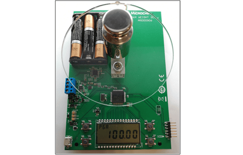
A high-accuracy weighing scale that can compensate for errors due to changes in temperature.

This reference design from Microchip is of a modular weighing scale that uses an automatic calibration process and techniques to minimize power consumption. The weighing scale features a digital display and a load cell to accurately measure the weight. The reference design is compact and has a low weight. The range and precision of the scale are user-defined and depend on the components selected while designing. The main advantage of this design
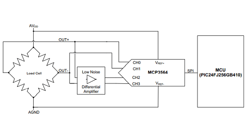
The reference design is based on the MCP3564 ADC, for enhancing the accuracy a temperature sensor can be added to the design. The design can precisely measure weight with a deviation of +/- 0.02g. The reference design offers a high gain and over-sampling ratio (OSR), moreover, the precision and accuracy of the design can be enhanced by using the external low-noise differential amplifier.
The reference design employs the PIC24FJ256GB410 microcontroller. The Extreme Low Power (XLP) feature of the microcontroller enables low power consumption, furthermore, the XLP application also includes an algorithm which switches the weight scale operating mode from Run mode to Sleep mode and an ultra-low power monitoring amplifier. The design can use either an external DC wall adapter or a Li-Ion battery as its power source.
The load cell is a transducer which converts an applied mechanical force into an electrical signal directly proportional to the magnitude of the force. The reference design employs four strain gauges as a load cell to measure the weight. Two strain gauge measure tension and the other two measure compression. These four strain gauges correspond to four resistors organized in a Wheatstone Bridge type of circuit as shown in the figure below:

The reference design uses the below formula to accurately measure the weight. The load cell gives a small voltage output, which is converted to the corresponding weight by the predefined algorithm. The formula used for calculating the output voltage is given below:

Features of the Reference Design:
- configurable OSR and gain
- high PSRR and CMRR
- differential analog inputs (this allows direct connection of the Wheatstone Bridge)
- differential reference voltage inputs • on-chip offset and gain calibration.
Microchip has validated this reference design and has also provided all the necessary design resources such as the BoM, Gerber file, schematics, software files, etc. to simplify the development of this reference design. You need to sign up to access the design files, you can get all the design resources here.


