


Electronic devices, microwaves and other household devices rely on PCB technology to stay in working condition.
Lifetime and performance of a PCB board depend on the choice of circuit board material. To select the right circuit board material, it is important to examine the materials available for different board categories. There are different properties and physical characteristics that help in the selection of board materials. While evaluating PCB Board materials, it is necessary to ensure that design requirements align with desired board capabilities.
Spacing and width of a board are also important, when it is required to handle high amounts of current. Structural strength of the board is defined by substrate and laminate. Selection of materials for these two layers is based on the type of board.

Layers in a PCB board and their significance
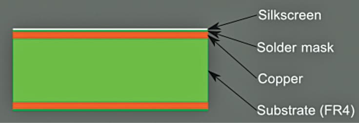
A PCB board consists of four layers, namely, substrate, laminate, solder mask and silkscreen. Together, the substrate and laminate define the basic electrical, mechanical and thermal circuit board properties.
Substrate
Fibre-glass FR4 is the most common material for the substrate of a PCB. Here, FR stands for fire retardant. It is suitable due to its rigidity and thickness. For flexible PCB, Kapton or equivalent property plastic is used.
Thickness of the PCB board depends on its application or use. For example, most Sparkfun products are 1.6mm thick, while Arduino Pro ones use 0.8mm thick boards. A PCB built with less expensive materials like epoxies lacks durability.
Substrates are found in low-cost consumer electronics. These have low thermal stability, which causes them to lose their lamination easily. Substrates can also cause smoke when a soldering iron is held for long on the board, which makes them easy to identify.
A non-conductive layer of the dielectric material is chosen based on dielectric constant.
Substrates must meet certain desired properties like glass transition temperature (Tg). Tg is the point where heat causes the material to deform or soften. There is a wide variety of materials available for substrates, such as aluminium or insulated metal substrate (IMS) FR-1 through FR-6, polytetrafluoroethylene (PTFE), CEM-1 through CEM-5, G-10 and G-11, RF-35, polyimide, alumina, and flexible substrates like Pyralux and Kapton.
Shavinder Singla, technical officer, Centre for Development of Advanced Computing, says, “IMS takes care of heat dissipation created by modern PCB designs, which are often linked to interconnection difficulties. Care must be taken while selecting IMSes for an application.
“In general, IMSes minimise thermal impedance and conduct heat more effectively. These substrates are mechanically more robust than thick-film ceramics and direct-bond copper constructions that are often used in many applications.”
Laminate
This provides properties like coefficient of thermal expansion, tensile and shear strength, and Tg. Common dielectrics used for laminates are CEM-1 and CEM-3, FR-1, FR-4, polytetrafluoroethylene (teflon), FR-2 through FR-6, CEM-1 through CEM-5, and G-10.
Copper foil is the next layer that is laminated to the board. For double-sided PCBs, copper is applied to both sides of the substrate. Copper’s thickness varies as per the application. For example, thickness is more for high-power applications, as compared to low-power ones.
Solder mask
This is the layer on top of the copper foil. It works as an insulation for copper traces from accidental contact with other conductive metals. It helps soldering at correct places.
It is a protective layer that guards against external contaminants and provides required isolation between surface elements like pads, copper traces and drill holes.
Silkscreen
Overlaid on top of the solder mask, a silkscreen is used to add letters, numbers and symbols to the PCB for easy assembly, and indicators to better understand the board.
Design technologies for PCBs
Each board serves a unique purpose for a particular product. Hence, it must be designed to perform that function in the allotted space. Designers use computer-aided design (CAD) systems with special software to lay out the circuit pattern on the board. Software available for PCB designs include Allegro PCB Designer, Altium Designer and PCB Droid. Use of software ensures that the design does not contain errors such as traces that are skinny or incorrectly touch, or drill holes that are tiny.
Ajay Singha, principal engineer, Lambda Consulting, opines, “Two most common design technologies for PCB designs are through-hole technology and surface mount technology (SMT). In the former, each component is pressed into tiny holes of the substrate and soldered to connect on the reverse side of the board.
“In SMT, L-shaped or J-shaped terminals of each component get in touch with the PCB directly.
“Components on a PCB are electrically connected to the circuit(s) by these methods. Although SMT eliminates the time-consuming drilling process and space-consuming connection pads inherent with through-hole technology, greater care is needed in the placement of components.”
An IC performs functions that are similar to those of a PCB, except that the IC contains many more circuits and components that are electrochemically grown in place on the surface of a tiny silicon chip.

A hybrid circuit contains some components that are grown onto the surface of the substrate rather being placed on the surface and soldered. It looks like a PCB.
Types of PCBs
Circuit boards may be classified in several ways, as follows:
- Component location: single-sided, double-sided and embedded
- Stack-up: single layer and multi-layer
- Design: module-based, custom and special
- Bendability: rigid, flex and rigid-flex
- Strength: electrically strong and mechanically strong
- Electrical functionality: high frequency, high power, high density and microwave
The board types can be used to select the circuit board material best suited for the design.
Single-sided PCBs include only one layer of a substrate, coated with a thin layer of copper. A protecting solder mask is laid down onto the copper layer. The silkscreen coat may be applied to the top to mark the elements of the board.
A double-sided PCB’s substrate includes metal conductive layers and elements attached to both sides (top and bottom).
Multi-layer PCBs enlarge the density and complexity of PCB designs by adding extra layers beyond the layers seen in the configuration of double-sided PCBs. These allow for extremely thick and highly-compound designs. Extra layers used are power planes that provide the supply to the circuit with power and decrease the levels of electromagnetic interference (EMI).
Rigid PCBs use a solid, rigid substrate material like fibre-glass that keeps the board from twisting. A motherboard within a computer is the best example of an inflexible PCB.
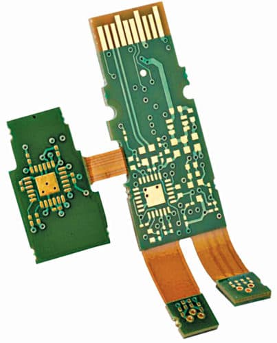
A flex PCB’s substrate is flexible plastic. It enables turning and shifting during use without harming the circuit(s) on the PCB. It can restore heavy wiring in superior gear where weight and space matter, such as satellites.
Rigid-flex boards consist of a rigid circuit board attached to a flex circuit board. These boards can fulfill compound design requests on demand.
Safety considerations for toxic materials
Fumes from the solder may contain lead, which is toxic. Solder is used to make electrical connections on a PCB, so soldering operations must be carried out in a closed environment. Fumes must be clean when being discharged into the atmosphere. One solution to replace the wires and solder is the use of water-soluble, electrically-conductive moulded plastics.
Thermal considerations for PCB board material selection
Two factors that impact PCBs are power and heat. Therefore it is crucial to determine the thresholds for each. This can be done by assessing the thermal conductivity of the PCBs through the length of the material.
PCB board material with low thermal conductivity causes heat, which can be a huge drawback for heat-intensive applications.
Selecting PCB board materials
PCBs are manufactured in single- as well as double-sided varieties, some of which are copper-clad and others use aluminium for military and aerospace, automobile and medical industries applications. For these specific areas, material used should give maximum performance.
PCB board materials are selected for their light weight, quality or their ability to handle high amounts of power. Since material levels correlate to performance levels, it is crucial to determine which functions need to be compared with one another when selecting PCB board materials.
Majority of flex boards consist of Kapton, a polyimide film that has qualities such as heat resistance, dimensional consistency and dielectric constant of only 3.6. Kapton comes in three Pyralux versions: FR, non-flame retardant (NFR) and adhesive-less, high performance (AP).
Quality is important in the construction of any type of board for home electronics or industrial equipment. Components such as PCBs should offer superior performance for the expected lifespan. Electronic devices, microwaves and other household devices rely on PCB technology to stay in working condition.
PCB for LED lighting
LED PCB boards generate heat while in operation. Hence, LED chips are mounted on a base made of metals like aluminium, copper or a mixture of alloy, and coated with high reflective surfaces to achieve optimum heat management and to increase light output. This keeps the heat-generating components cool and improves their ability to dissipate heat. This results in increased performance and life of the LEDs.
Consequently, metal-core PCBs (MC-PCBs) are chosen for LED applications. These include a thin layer of thermally-conductive dielectric material that can transfer and dissipate heat with much greater efficiency than traditional rigid-PCBs. FR-4 materials include a thermal aluminium-clad layer to efficiently dissipate heat. Whereas, MC-PCB board materials are developed for higher power.
The future
Miniaturisation of electronic products continues to drive PCB manufacturing towards smaller and more densely-packed boards with increased electronic capabilities. Advancements include 3D moulded plastic boards and increased use of IC chips. Such advancements will keep the manufacture of PCBs a dynamic field for years to come.
Planning a well-designed layer stackup can both minimise electromagnetic radiation and stop circuits from being interfered by external noise sources. It can also reduce signal crosstalk and impedance mismatch issues. Development of modern electronics demands new PCB features such as lightweight, miniaturisation, better functionality and reliability, high speed, and longer life.