Introduction
Shrinking the size of the power solution often sits among the top priorities on a system engineer’s list. This is not because it is a very attractive feature, but because the engineer needs the space on the already crowded PCB to accommodate the product’s main selling features. Power solution providers have been working to minimize the power solution on many fronts. One of their techniques has been to integrate the cumbersome external feedback compensation network into the IC via an approach called internal compensation.
Internal compensation doesn’t come for free. It can affect the power solution loop’s bandwidth and stability. This article examines different internal compensation techniques, one of which offers wide loop bandwidth, achieving high integration without the loop’s bandwidth and stability tradeoffs.
Internal compensation techniques
Simple internal compensation
Figure 1 shows a typical power supply circuit with its feedback loop and external compensation circuit. The compensation circuit is optimized to a specific operating condition (input voltage, output voltage, switching frequency, and output capacitor). When one or more of the circuit operating parameters changes, the compensation circuit value(s) must be changed to optimize the loop performance according to the new circuit operating condition.

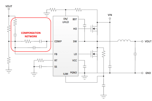
Simple internal compensation essentially integrates this compensation circuit, which is optimized for one specific operating condition, into the IC. The IC with this internal compensation circuit would work just fine, until one or more operating parameter(s) changes. Figure 2 shows a power solution with simple internal compensation.
The internal compensation is optimized for one specific operating condition. This converter works great at this specific operating condition, but it is also limited to this operating condition. Its performance degrades when the operating condition changes, e.g. changing Vo, Fsw, and/or Co values.
Smart, wide-bandwidth internal compensation
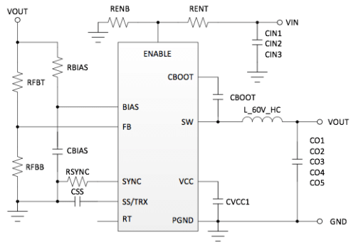
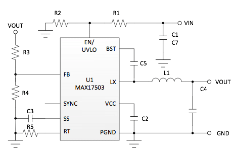
Figure 3 shows the schematic of a buck converter which employs smart, wide-bandwidth internal compensation. This technique allows adjustment to suit different circuit conditions and retains optimized loop bandwidth for a wide range of operating circuit parameters. And, of course, it minimizes the number of external components to provide a highly integrated, compact power solution.
Smart versus simple internal compensation
Simple internal compensation example
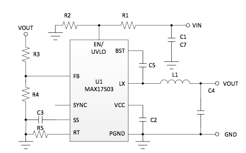
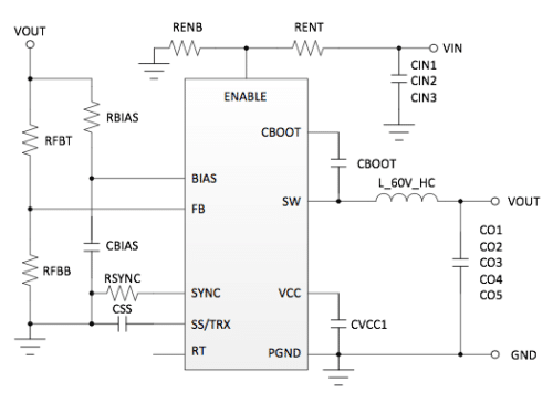
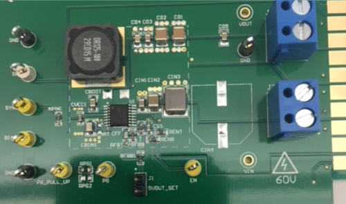
In contrast to the previously discussed buck converter with wide-bandwidth internal compensation, here is an example of a buck converter implementing a simple internal compensation technique. Its schematic, evaluation board, and BOM are listed in Figures 4a and 4b and Table 1.
| Designator | Description | Quantity |
| C04, C05 | CAP, CERM, 0.022μF, 100V, +/-5%, X7R, 0805 | 2 |
| CBIAS | CAP, CERM, 4.7μF, 50V, +/-10%, X5R, 0805 | 1 |
| CBOOT | CAP, CERM, 0.47μF, 16V, +/-10%, X7R, 0805 | 1 |
| CFF | CAP, CERM, 100pF, 50V, +/-5%, C0G/NP0, 0603 | 1 |
| CIN1 | CAP, CERM, 0.47μF, 100V, +/-10%, X7R, 0805 | 1 |
| CIN2 | CAP, CERM, 1μF, 100V, +/-10%, X7R, 1210 | 1 |
| CIN3 | CAP, CERM, 10μF, 100V, +/-20%, X7S, 2220 | 1 |
| CO1, CO2 | CAP, CERM, 47μF, 10V, +/-10%, X7R, 1210 | 2 |
| CO3 | CAP, CERM, 1μF, 25V, +/-10%, X5R, 0805 | 1 |
| CSS | CAP, CERM, 0.047μF, 50V, +/-10%, X7R, 0603 | 1 |
| CVCC1 | CAP, CERM, 2.2μF, 10V, +/-10%, X7R, 0603 | 1 |
| L_60V_HC | Inductor, shielded drum core, ferrite, 10μH, 5.35A, 0.0189 ohm, SMD, Coiltronics DR125-100-R 1 | 1 |
| Misc. Resistors | 0603 | 8 |
| U1 | 3.5- 60V 2A step-down converter | 1 |
Table 1. BOM for buck converter with simple internal compensation
This particular buck converter employs fixed-frequency peak current mode control. The device is internally compensated. The switching frequency is programmable from 200kHz to 2.2MHz by an external resistor, RT. It defaults at 500kHz without RT. The internal compensation is optimized for: 24V input, 3.3V output, 500kHz switching frequency, and output capacitor of 2x47uF ceramic. This converter works great at this specific operating condition, but it is also limited to this operating condition. Its performance degrades when the operating condition changes, e.g. changing Vo, Fsw, and/or Co values.
To demonstrate the limitation of simple internal compensation, let’s observe the converter’s responses to load step transient at various circuit operating conditions. Figure 5a shows a test result with original configuration (2x47uF), while Figure 5b shows the result with twice the amount of output capacitor (4x47uF).
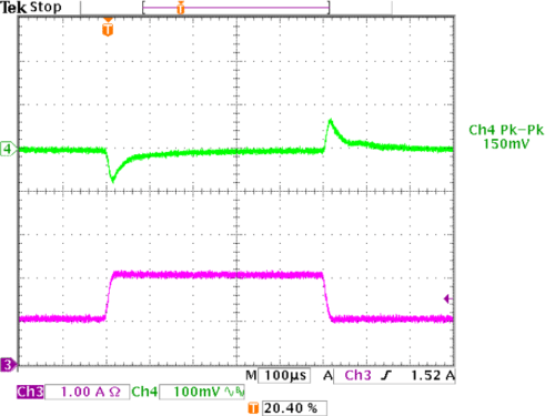
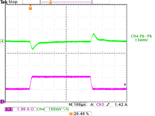
The purple trace is the output load current stepping from 1A to 2A and back to 1A. The green trace is the output voltage showing deviation in response to the load changes. An ideal converter would have no voltage deviation when the load changes (i.e. the green line is flat). A faster converter has less voltage deviation. A stable converter has a well-behaved output voltage waveform that recovers smoothly from the deviation.
This original circuit (2x47uF) has a 150mV peak-to-peak (pk-pk) voltage deviation. When doubling the output capacitor to 4x47uF, we would expect the voltage deviation to be reduced to half. However, due to the limitation of simple internal compensation, increases in the output capacitance consequently reduce the converter loop bandwidth, thus adversely affecting the converter performance. Therefore, we measured 134mV pk-pk in this case.
So, with simple (limited) internal compensation, doubling the output capacitance only reduces the output load transient response peak to peak slightly to 89%. This 11% reduction figure doesn’t justify the cost and size increase for adding the output capacitor. As a system engineer, you are stuck with the original converter performance. Trying to improve output voltage deviation performance further incurs exponential cost and size increases.
Smart, wide-bandwidth internal compensation example
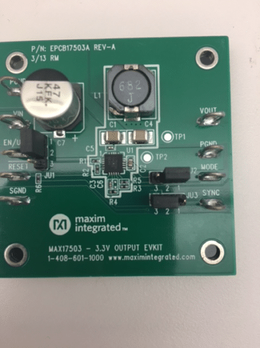
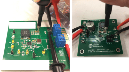
Figure 6a and 6b and Table 2 shows the schematic, evaluation kit board, and BOM of the buck converter with smart, wide-bandwidth internal compensation.
| Designator | Description | Quantity |
| C1 | 2.2μF ±10%, 100V X7R ceramic capacitor (1210) | 1 |
| C2 | 2.2μF ±10%, 10V X7R ceramic capacitor (0603) | 1 |
| C3 | 5600pF ±10%, 25V X7R ceramic capacitor (0402) | 1 |
| C4 | 47μF ±10%, 10V X7R ceramic capacitor (1210) | 1 |
| C5 | 0.1μF ±10%, 16V X7R ceramic capacitor (0402) | 1 |
| C7 | 47μF, 80V aluminum electrolytic capacitor (D = 10mm) | 1 |
| L1 | 6.8μH, 5A inductor. Coilcraft MSS1048-682NL. Taiyo Yuden NS10165T6R8NNA |
1 |
| Misc Resistors | 0402 | 5 |
| U1 | 4.5V-60V, 2.5A, high-efficiency, synchronous step-down DC-DC converter with internal compensation | 1 |
Table 2. BOM for buck converter with wide-bandwidth internal compensation.
This particular converter is also a fixed-frequency peak current mode control device. However, it features smart, wide-bandwidth internal compensation. The switching frequency of its evaluation kit is defaulted to 450kHz. The internal compensation is optimized for: 24V input, 3.3V output, 450kHz switching frequency, and output capacitor of 47uF ceramic. Let’s note that this is only half the amount of the output capacitance on the other board discussed earlier. We’ll see later that this buck converter requires only half of the amount of output capacitance for a comparable output transient response because of its wide loop bandwidth.
To examine the performance of smart, wide-bandwidth internal compensation, let’s observe the converter responses to load step transient at various circuit operating conditions. Figure 7a shows a test result with the original configuration (47uF), while Figure 7b shows the result with twice the amount of output capacitor (2x47uF).
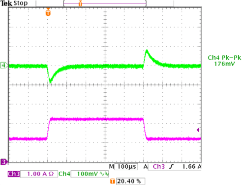
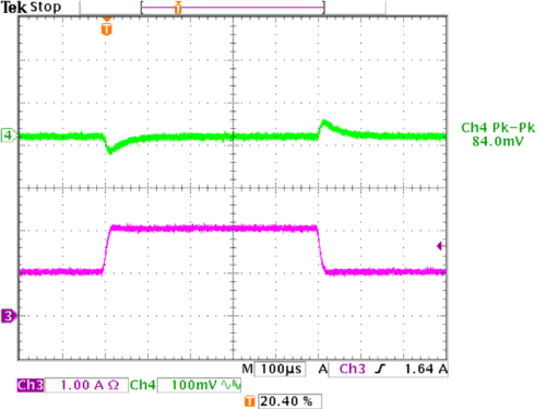
The original circuit (47uF) has a 176mV pk-pk voltage deviation. When doubling the output capacitor to 2x47uF, the voltage deviation reduces to 48% at 84mV pk-pk thanks to its smart, wide-bandwidth internal compensation. The well-behaved recovering wave shape of the output voltage after each deviation also indicates very stable loop operation. Furthermore, this converter requires only half of the amount of output capacitance for a comparable output transient response because of its wide loop bandwidth, when compared to the simple internal compensation solution.
Table 3 shows a side-by-side comparison of the simple internal compensation buck converter with the option featuring smart, wide-bandwidth internal compensation.
| Simple Internal Compensation |
Smart, Wide-Bandwidth Internal Compensation | |||
| Output Capacitance | Vo Deviation, pk-pk | Output Capacitance | Vo Deviation, pk-pk | |
| Original Configuration | 2x47uF | 150mV | 47uF | 176mV |
| Doubling Output Capacitance | 4x47uF | 134mV | 2x47uF | 84mV |
| Percentage Vo Deviation Reduction | 11% | 52% | ||
Table 3. Comparing two types of buck converters.
It should be noted that when measuring output voltage load transient response, a low-noise scope probe must be used. Figure 8 shows what was used to measure these voltages. Equipment used in this experiment includes: power supply-HP6032A, electronic load – Agilent 6060B, and oscilloscope – Tektronix TDS3034B. Load step slew rate: 1A/us, output voltage probe bandwidth, Ch4: 20MHz, output current probe bandwidth, Ch3: 300MHz.
Summary
Internal compensation helps reduce external component count and circuit complexity for higher integration power solutions. Simple internal compensation trades off the benefits with lower system performance and also might cause loop instability. Smart, wide-bandwidth internal compensation, which is available in the MAX17503, achieves the best of both worlds: high integration while maintaining optimum loop bandwidth and control loop stability, reducing size and cost by reducing the external output capacitance requirement.