


 There are at least twelve simple experiments that can be performed using IC 555 and simultaneously learn the theory and digital logic behind its operation. Here you will find the first six experiments and the rest will be provided in second part of this article to follow soon.
Although these circuits are experimental and non-conventional, they help in understanding the IC that comprises a voltage divider, trigger comparator, threshold comparator, SR flip-flop, discharge transistor, reset transistor, and the output stage. These also help in understanding its three modes of operation: monostable, astable, and bistable.
All the experiments are simple and can be performed on a breadboard. A power supply of 5V to 9V DC may be used for all the circuits (although, according to its data sheet 4.5V to 15V can be used). The operation of all the twelve experiments is confirmed by the glowing of LEDs.
In the first experiment only a part of the internal circuitry of the IC is used. In second, third, and fourth experiments output pin 3 of the IC 555 is not used but the monostable, astable, and bistable operations using internal two comparators and an SR flip-flop occur, as they normally occur, and their performance is demonstrated by the LEDs. In the fifth and sixth, two 555 ICs are used to create an interesting situation. The experiments make the learning of IC 555 an enjoyable experience.
Experiment 1
Circuit diagram for conducting the first experiment is shown in Fig. 1. It has three sections: 1(a), 1(b), and 1(c).
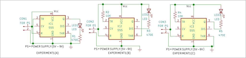
For experiment 1(a), pin numbers 4 and 8 of the IC are connected to the (5V to 9V) power supply Vcc, while pins 1, 2, and 6 are grounded. The LED is connected between pin 3 and ground through current-limiting resistor R1. When the circuit is powered, LED1 turns on and glows continuously. Here only the lower comparator and output stage of the IC are used.
For experiment 1(b), pin numbers 4, 6, and 8 of the IC are connected to the power supply; pin 2 is connected to the power supply through resistor R2. Pin 1 is grounded. LED2 is connected between Vcc and pin 7 through current-limiting resistor R3. When the circuit is powered, LED2 turns on and glows continuously. Here only the upper comparator and the discharge transistor of the IC are used.
For experiment 1(c), pin numbers 4 and 8 of the IC are connected to the power supply; pin 2 is connected to Vcc through resistor R4. Pins 1 and 6 are grounded. LED3 is connected between Vcc and pin 3 through current-limiting resistor R5. When the circuit is powered, LED3 turns on and glows continuously. Here only the output stage of the IC is used.
Experiment 2
Circuit diagram for the second experiment is shown in Fig. 2. Here the IC is wired as a monostable multivibrator.
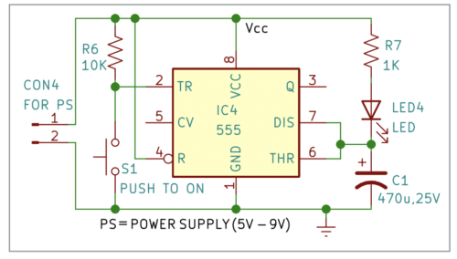
A blue-coloured LED4 is connected between resistor R7 and capacitor C1. When the circuit is powered, LED4 glows as it gets grounded through the internal discharge transistor at pin 7. However, capacitor C1 cannot charge. When S1 is pushed momentarily, the capacitor starts charging through R7 and LED4.
As the capacitor starts charging, it pulls the charge through LED4 and the LED starts fading as the voltage across it drops. When the capacitor voltage exceeds two-third of Vcc, it discharges through pin 7 because of internal comparators as per normal monostable operation and LED4 glows again.
Though output pin 3 is not used, the monostable operation of the circuit is visible through the fading and glowing of LED4.
Experiment 3
The circuit diagram for experiment 3 is shown in Fig. 3. Here the IC is wired as an astable multivibrator so that the two LEDs, LED5 and LED6, flash and fade alternately.
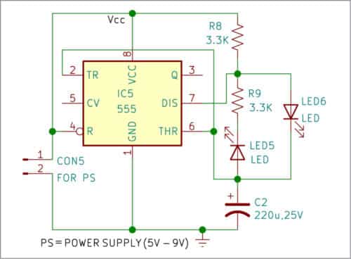
Capacitor C2 charges through resistor R8 and LED6 and discharges through LED5 and resistor R9, causing the LEDs to flash and fade alternately. The flashing and fading of the LEDs show the charging and discharging of capacitor C2, which occurs because of the IC’s internal comparators as per normal astable operation. LED5 and LED6 are 5mm, transparent bright-green LEDs. Thus, without connecting any load to output pin 3 of the IC, its astable operation can be observed.
Experiment 4
Circuit diagram for the fourth experiment is shown in Fig. 4. Here the IC is wired as a bistable multivibrator.
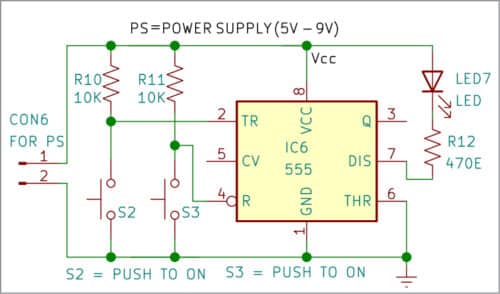
In this circuit, the LED is connected between Vcc and pin 7 of the IC through current-limiting resistor R12. In conventional bistable operation, the discharge pin 7 of IC 555 is not used as the circuit has no capacitor.
Initially, when the circuit is powered, LED7 turns on. When switch S2 is pushed, LED7 turns off, and when switch S3 is pushed, it turns on. This is just the reverse of the conventional bistable operation as instead of output pin 3, discharge pin 7 is used.
In this circuit the function of the internal discharge transistor (pin 7) can be visibly seen through LED7. Normally, pin 7 of the IC is used to discharge the capacitor when the IC is operating as an astable or a monostable multivibrator.
Experiment 5
Circuit diagram for experiment 5 is shown in Fig. 5. Here two ICs, IC7 and IC8, are used. IC7 is wired as a monostable multivibrator and IC8 is wired as a bistable multivibrator.
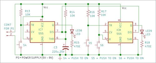
Discharge pin 7 of both the ICs are connected together. Initially, when the circuit is powered, the output at pin 3 of IC7 and IC8 is low and both LED8 and LED9 are off.
When switch S4 is pushed, LED8 turns on and stays on continuously, though the circuit is wired as a monostable multivibrator. This is because capacitor C3 is shorted to ground by the internal discharge transistor pin 7 of IC8. Due to this capacitor C3 cannot charge and the monostable operation fails to occur.
In the same situation, when switch S5 is pushed, LED9 turns on and stays on continuously. At the same time, the monostable operation of IC7 is resumed and LED8, which was continuously on initially, turns off after the predetermined time decided by resistor R14 and capacitor C3.
When switch S6 is pushed, LED9 turns off. This is a normal bistable operation. Thus, both LED8 and LED9 stay off in the same manner when the circuit is initially powered.
Experiment 6
Circuit diagram for experiment 6 is shown in Fig. 6. Here, two ICs, IC9 and IC10, are used. IC9 is wired as an astable multivibrator and IC10 is wired as a bistable multivibrator. In this circuit also discharge pin 7 of both the ICs are connected together.
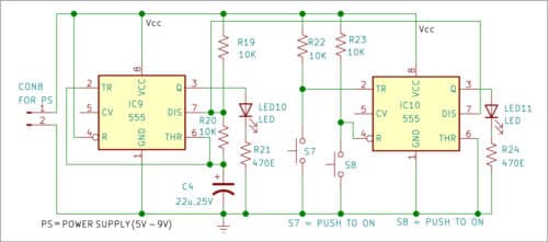
Initially, when the circuit is powered, LED10 turns on and stays on continuously, though the circuit is wired as an astable multivibrator. This is because capacitor C4 is shorted to ground by the internal discharge transistor pin 7 of IC10. Due to this capacitor C4 cannot charge and the astable operation fails to occur.
| Part List | |
| Semiconductors: | |
| IC1-IC10 | – IC555 timer |
| LED1-LED3, | – 5mm white |
| LED7-LED11 | transparent LED |
| LED4 | – 5mm blue LED |
| LED5-LED6 | – 5mm bright green transparent LED |
| Resistors (all 1/4-watt, ±5% carbon): | |
| R1, R3, R5, R12, R15, | |
| R18, R21, R24 | – 470-ohm |
| R2, R4, R6, R10, R11 | |
| R13, R14, R16, R17, | |
| R19, R20, R22, R23 | – 10-kilo-ohm |
| R7 | – 1-kilo-ohm |
| R8-R9 | – 3.3-kilo-ohm |
| Capacitors: | |
| C1 | – 470µF, 25V electrolytic |
| C2, C3 | – 220µF, 25V electrolytic |
| C4 | – 22µF, 25V electrolytic |
| Miscellaneous: | |
| CON1-CON8 | – 2-pin connector |
| S1-S8 | – Push-to-on switch |
| PS | – 9V battery/0-12V variable power supply |
| – Bread board 1 or 2 | |
When switch S7 is pushed, LED11 turns on and remains on until switch S8 is pushed. This is a normal bistable operation. However, when S7 is pushed, LED10 that was on continuously starts blinking on and off as the astable operation starts.
When switch S8 is pushed, LED11 turns off and LED10, which was blinking on and off, stays on continuously again as explained earlier, until S7 is pushed again.
All these circuits can be wired on a breadboard so that the components can be reused, if required. A variable 0-12V, 1A power supply can be used for the experiments. Alternatively, you can use a 9V battery. Connectors CON1 through CON8 are used to connect power supply/battery.
Read Part 2
Rajeev Nilkanth Deshpande is M.Sc. in chemistry and has been pursuing electronics as a hobby for over 47 years.

Did this on proteus simulation. !
Part list having missed resistor valves for the following reference designators
R1, R3, R5, R12, R15, R2, R4, R6, R10, R11, R13, R14, R16, R17
Dear Sir,
All values are given such as :
R1, R3, R5, R12, R15,
R18, R21, R24 all have 470 E. Similarly others are also given.