


 The first six circuits to learn the theory and digital logic behind twelve simple experiments that can be performed using IC 555 were published in Part 1. Here are the remaining six circuits.
Although the circuits are non-conventional, they help understand the IC 555 comprising a voltage divider, trigger comparator, threshold comparator, SR flip-flop, discharge transistor, reset transistor, and output stage.
They also help understand the IC’s three modes of operation:
- Monostable
- Astable
- Bistable
The visible operation of the IC in all twelve experiments is shown by LEDs.
All the experiments are simple and can be performed on a breadboard. A power supply of 5V to 9V DC can be used for the circuits (although according to the datasheet of IC 555, 4.5V to 15V may be used).
In the following circuits, two 555 ICs are used to create interesting situations and make learning an enjoyable experience.
Experiment 7
As shown in Fig. 7, in this circuit both the ICs, IC12 and IC13, are wired as bistable multivibrators. However, the output pin 3 of each IC is connected to the discharge pin 7 of the other IC through an LED and a current limiting resistor. In normal bistable operation, discharge pin 7 is not used as there is no capacitor in the circuit.
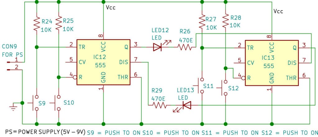
Initially, when the circuit is powered, both LED12 and LED13 remain off. When switch S9 is pressed, LED12 turns on, and when S10 is pressed, LED12 turns off. Similarly, when S11 is pressed, LED13 turns on, and when S12 is pressed, LED13 turns off. This is a normal bistable operation.
But if switch S9 is pressed to switch on LED12 and then S11 is pressed, instead of LED13 turning on LED12 turns off. Thus, both LED12 and LED13 remain off though the output at pin 3 of both the ICs is high! This unique situation arises because the internal discharge transistors at pin 7 of both the ICs turn off and the transistors cannot conduct.
Now, in this situation, if S10 is pressed, LED13 turns on, and it is on-and-off operation can be controlled by S9 and S10. Likewise, the on-and-off operation of LED12 can be controlled by S11 and S12. However, both LEDs can never be on together.
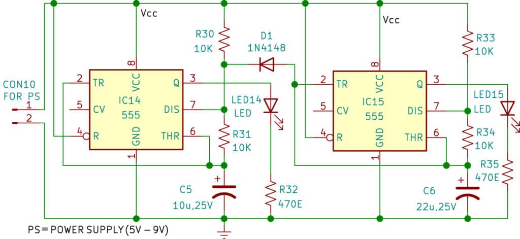
Experiment 8
The circuit diagram for the eighth experiment, shown in Fig. 8, has two parts: 8(a) and 8(b).
In part 8(a) both the ICs are independently wired as astable multivibrators. They are identical, except the value of C5 is lower than that of C6. Normally, if the ICs are powered separately, both LED14 and LED15 flash, but the flashing of LED14 is faster than that of LED15.
However, in this circuit diode, D1 is connected between pin 7 of IC14 and capacitor C6. So, when the circuit is powered, LED14 flashes but LED15 stays on continuously. This is because capacitor C6 keeps discharging through pin 7 of IC14 through diode D1 and the astable operation of IC15 fails to occur.
Now, if the orientation of diode D1 is reversed (cathode of diode connected to pin 7 of IC15 and anode to the positive end of capacitor C5), both LED14 and LED15 start flashing, though LED14 flashes at a slower rate as capacitor C5 intermittently discharges through pin 7 of IC15.
In part 8(b) the two ICs are again independently wired as astable multivibrators. The output from pin 3 of both the ICs is commonly connected to LED16 through diodes D2 and D3. When the circuit is powered, LED16 ‘seems’ to glow continuously.
However, in fact, LED16 is powered alternately by two independent astable multivibrators continuously.
When the on/off switch S13 is closed, LED16 turns off as the circuit resets. If it is opened, LED16 glows immediately as the astable multivibrator operation is self-triggering. So, the circuit with two independent astable multivibrators together ‘appears’ to act as a bistable multivibrator!
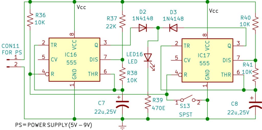
Experiment 9
As shown in Fig. 9, in this experiment both the ICs are once again wired as astable multivibrators. They are identical, except capacitor C9 is of a much lower value than capacitor C10. When powered independently, LED17 flashes fast and LED18 flashes slowly.
In this circuit, pin 5-a voltage control pin—is used. This pin is rarely used, and when not used, it is generally grounded through a 0.01µF capacitor.
Here, pin 3 of IC18 is connected to pin 5 of IC19. When the circuit is powered, both LED17 and LED18 flash fast, almost synchronously. This is because the output square wave of the IC18 astable multivibrator with higher frequency overrides and modulates the square wave of the IC19 astable multivibrator with a lower frequency through pin 5.
Now, if the situation is reversed and output from pin 3 of IC19 is connected to pin 5 of IC18, the phenomenon gets reversed. The flashing of both LED17 and LED18 starts. The flashing of LED17 is faster than that of LED18, the latter appears to be steady but soon both the LEDs turn off synchronously for some time and the cycle continues.
Experiment 10
In the tenth experiment, as shown in Fig. 10, IC21 is wired as a simple oscillator. The internal voltage divider of IC20, consisting of three 5k resistors in series that internally create reference voltages for the internal comparators, is used here in part as a resistive path to charge and discharge capacitor C11.
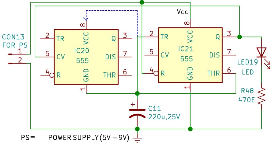
Pin 3 of IC21 is connected to pin 5 of IC20. Pins 2 and 6 of IC21 that are tied together are connected to pin 1 of IC20. When the circuit is powered, LED 19 flashes. If pins 2 and 6 of IC21 are connected to pin 8 of IC20 instead of pin 1 of IC20, the flashing rate of LED19 increases, as the resistance decreases.
Experiment 11
In the circuit for this experiment, shown in Fig. 11, IC22 is wired as a monostable multivibrator and IC23 as an astable multivibrator. Pin 8 of IC23, instead of connecting to Vcc, is connected to pin 3 of IC22.
When switch S14 is momentarily pushed, the output of pin 3 of IC22 goes high and powers IC23. Both the capacitors C12 and C13, which are identical, start charging almost simultaneously.
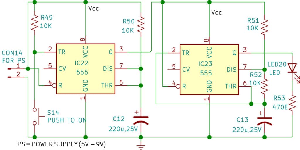
However, the charging of C13 is comparatively slower as it charges through two resistors in a series. The LED20 turns on but before C13 gets a chance to charge to more than 2/3 of Vcc, C12 charges to more than 2/3 of Vcc, and IC22, which is wired as a monostable multivibrator, completes its one-shot cycle and its output goes low and LED22 turns off.
So, although IC23 is wired as an astable multivibrator, it is very first cycle remains incomplete. Thus, both the ICs together ‘appear’ to act as a monostable multivibrator!
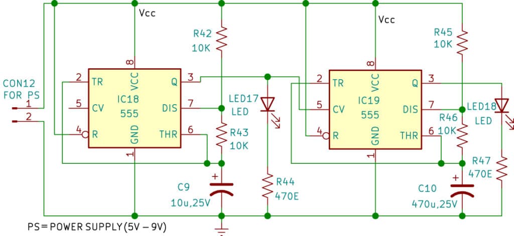
| Parts List | |
| Semiconductors: | |
| IC12-IC27 | – Timer IC 555 |
| LED12-LED23 | – 5mm LED |
| D1-D5 | – 1N4148 signal diode |
| Resistors (all 1/4-watt, ±5% carbon): | |
| R24, R25, R27, R28, | |
| R30, R31, R33, R34, | |
| R36, R38, R40-R43, | |
| R45, R46, R49-R52, | |
| R54, R57, R60, R63, | |
| R64 | -10-kilo-ohm |
| R26, R29, R32, R35, | |
| R39, R44, R47, R48, | |
| R53, R56, R59, R62 | – 470-ohm |
| R37 | – 22-kilo-ohm |
| R55, R58, R61, R65 | – 47-kilo-ohm |
| Capacitors: | |
| C5, C9 | – 10µF, 25V electrolytic |
| C6-C8, C16-C19 | – 22µF, 25V electrolytic |
| C10 | – 470µF, 25V electrolytic |
| C11, C12, C13 | – 220µF, 25V electrolytic |
| Miscellaneous: | |
| CON9-CON16 | – 2-pin connector |
| S9-S12, S14-S17 | – Push-to-on switches |
| S13 | – SPST (ON/OFF switch) |
| PS | – 9V battery/0-12V variable power supply |
| – Breadboard | |
Experiment 12


waiting
Part list having missed resistor valves for the following reference designators
R24, R25, R27, R28, R30, R31, R33, R34, R36, R38, R40-R43, R45, R46, R49-R52, R54, R57, R60, R63, R26, R29, R32, R35, R39, R44, R47 and R48
Dear Sir,
All values are given such as :
R24, R25, R27, R28,
R30, R31, R33, R34,
R36, R38, R40-R43,
R45, R46, R49-R52,
R54, R57, R60, R63,
R64 all are 10-kilo-ohm. Similarly others are also given