


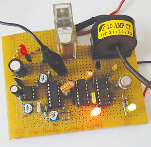
 There are occasions when the water pump runs idle when there is no water in the sump/underground tank or the treadmill machine is left on, unintentionally. In such cases, motors of these electrical machines run unnecessarily. Running these for a long time may lead to burnout. Such situations can be addressed by using this no-load and overload protector circuit. It can switch off the appliance in case of overload. The author’s prototype is shown in Fig. 1.
Circuit and working
Circuit diagram of the no-load and overload protector for the AC motorised circuit is shown in Fig. 2. It is built around NE555 timer (IC1), decade counter 4017 (IC2), quad comparator LM339 (IC3), quad NOR gate CD4001 (IC4), current transformer (CT1), transistors BC547 (T1, T3, T4) and SL100 (T2), and a few other components. The circuit works off a 12V DC supply. You can use a 12V, 1A SMPS unit at connector CON1.
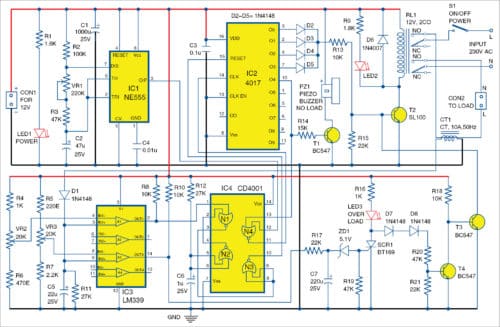
Clock signal is provided to decade counter 4017 (IC2) from the astable multivibrator wired with timer NE555 (IC1) through NOR gate N4. Other input of N4 is fed from Q4 output of IC2. If Q4 of IC2 is low, clock pulse enters counter IC2.
In a normal situation, Q4 of IC2 will be at low state, except for no-load condition. Q0 output of IC2 will be high if reset pin 15 of IC2 is in high state. When reset pin 15 is in low state, it allows the counter to count, so each output (Q0 through Q3) will change the state from low to high, sequentially. All four outputs (Q0 to Q3) are logically ORed and used to drive T2 and energise relay RL1.
If Q4 of IC2 becomes high, NOR gate N4 will not allow the clock pulse to enter the counter. So, T2 will be off and RL1 will be de-energised. This condition will continue till the next power supply restarts.
The amount of load current to the motorised electrical gadget is sensed by the coil of 50Hz, 10A current transformer (CT1) in the form of AC voltage. Sampled AC voltage in CT coil is proportional to the load current of the electrical gadget. This 50Hz AC voltage across the coil is rectified and filtered to get corresponding DC sample voltage. DC sample voltage is compared with reference voltages derived through two resistive networks in two comparators, A1 and A3, of LM339 (IC3).
In normal load condition, voltage from potmeter VR2 (which is used for checking no-load condition) should be set marginally less than the sample DC voltage. This provides high output at pin 2. If load current reduces, reference voltage from VR2 goes higher than the sample voltage, and output of A1 at pin 2 becomes low.
In normal load condition, reference voltage from VR3 is set adequately higher than the sample DC voltage. This gives low output at pin 14 of A3. If an overload condition arises, sample voltage goes higher than reference DC voltage, and output at pin 14 of A3 becomes high.
Gate N2 of IC4 is wired as a NOT (inverter) gate for making an initial reset pulse circuit with RC network formed by R12 and C6. This reset circuit is essential to reset counter IC2 on initial power on, so that output Q0 of IC2 becomes high and switches on T2. This, in turn, energises relay RL1 to provide AC power to the load.
DC sample voltage from the rectifier is available at cathode of D1. It is used for comparison and logical operation of gates. Normally, output of A3 at pin 14 is low, and capacitor C7 is in discharged state. Zener diode ZD1 will not conduct, and SCR1 will be cut-off. T4 switches on as it gets base bias through R16, LED3, D7, D8 and R20.
T3 goes off as its base is grounded through T4. Off state of T3 will not pull down the base bias voltage of T2. T2 is controlled by the output levels from Q0 to Q3 of IC2. The table shows the truth of NOR gate.

Operation of the circuit under different load conditions
Normal-load current condition
In this condition, DC sample voltage from the rectifier at pins 5 and 9 of IC3 are more than its reference voltage at pin 4, and less than its reference voltage at pin 8. Since load current differs for various electrical gadgets, for example, different horse power rated motors of water pumps, reference voltages at pins 4 and 8 have to be set using VR2 and VR3 for no-load and overload conditions, accordingly.
Output at pin 2 of IC3 is high, and output at pin 14 is low (after initial reset time delay). N1 output at pin 3 of IC4 is low and inverted output at pin 10 of N3 is high. This high condition keeps IC2 in reset state. Q0 is high and counter IC2 does not progress. High Q0 is used to switch on T2 and energise RL1. This connects AC mains power to the load through relay contacts. In this condition, T3 is cut off and maintains base bias of T2 as high.
No-load or low-load current condition
In this condition, DC sample voltage from the rectifier at pin 5 is less than the reference voltage at pin 4 from VR2. Output of A1 at pin 2 of IC3 becomes low and output of N1 at pin 3 of IC4 becomes high. Inverted output at pin 10 of N3 becomes low. Reset pin 15 of IC2 becomes low. This allows the counter to progress through Q1, Q2, Q3 and Q4. Here, Q0 to Q3 are ORed and used to drive T2, so that T2 conducts till counter output reaches Q4.
This mechanism is provided to establish sufficient delay before cutting off the supply to the load. This delay can be adjusted by changing the frequency of astable multivibrator IC1 by adjusting the value of potmeter VR1. Once Q4 becomes high and drives T1, the piezo buzzer (PZ1) is switched on. The high Q4 is fed to pin 13 of NOR gate N4, which blocks the clock pulses of IC2 at pin 14. Functioning of counter IC2, logical circuits and comparators freezes till next switching off and on of AC mains supply using switch S1.
If 12V SMPS is used, its input supply should be taken through switch S1.
Overload or short-circuit condition
In this condition, DC sample voltage from rectifier at pin 9 goes more than the voltage across VR3. Output of A3 at pin 14 changes from low to high. This high level is applied across reverse-biased Zener diode ZD1 through an integrator formed by resistors R10 and R17, and capacitor C7. This integrator network and Zener diode provide sufficient time delay to fire SCR1 through its gate. Time delay is required to avoid unwanted tripping off the load by initial in-rush current to inductive load or occurrence of any brief overload condition.
In case SCR1 is fired due to prolonged (more than delay time imposed by integrator and Zener diode) overload condition, anode potential of SCR goes less than one volt. This small anode voltage is not sufficient to forward bias diodes D7 and D8, which, in turn, cut off T4. Cut off condition of T4 makes T3 switch on, and its collector potential to come down to ground potential. This, in turn, pulls down base bias of T2, leading it to cut off. This leads to de-energising RL1 and withdrawal of mains supply to load.
Once SCR1 is fired and starts conducting between cathode and anode, status continues till the power switches off and on again. LED3 (initially dim) glows bright, indicating the registered status of overload condition till next restart. Withdrawal of power supply to load by RL1 establishes a no-load condition. The no-load sensing circuit starts to act, and audio alarm sounds from buzzer PZ1.
Initial reset and extending power supply to load
When power supply is initially switched on, 12V SMPS/12V DC extends DC supply voltage to the circuit. High output of counter may not be between Q0 and Q3. So, T1 and RL1 should not be energised until reset pin 15 of IC2 becomes high. In the beginning, no-load comparator A1 of IC3 gives low output, and output of gate N2 is high till voltage across C6 reaches an adequate level to change the output state of N2 to low.
Reset delay network comprises R12, C6 and N2. In the beginning of switch-on phase, input of gate N1 is high and low, and it gives low output. This is inverted by N3 to high, which resets IC2. Now, Q0 of IC2 becomes high and drives T1 and energises RL1.
Construction and testing
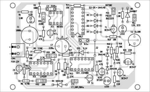
An actual-size PCB layout of the no-load overload protector for the motorised circuit is shown in Fig. 3 and its components layout in Fig. 4.

Download PCB and Component Layout PDFs: click here
Connect 12V SMPS or 12V DC to the circuit and enclose the PCB in a suitable PVC box. Since AC mains is used, use connectors with proper ratings and wires for AC input and output. Place the LEDs for power, normal output and overload in the front panel of PVC box. Make a hole on the box for the buzzer to indicate output tripped-off condition. Extend earth wire from AC mains to the load through the box.
To carry out no-load and overload alignments, measure sample voltage from the rectifier at cathode of D1 using a digital multimeter. A window of sample voltage for safe operation of an electrical circuit must be decided with an upper limit and lower limit. Adjust VR2 to lower limit voltage across its variable arm and ground, and adjust VR3 to upper limit voltage across its variable arm and ground.
For example, if the rectifier is providing a DC sample voltage of 6V on normal-load condition, you can decide the window between 5V and 8V. (Since sufficient delay is provided for no-load condition, any instantaneous or brief no-load conditions will not affect the normal operation of the circuit.) Set the voltage across variable arm of VR2 and ground to 5V, and voltage across variable arm of VR3 and ground to 8V.
Current transformer
Basic primary current is 1A, and maximum primary current is 10A. Operating frequency is 50Hz, while winding ratio is 1:1200.

Notes
- Only live (phase) wire of load side should be passed through the current transformer (CT1).
- You can use 12V, 1A SMPS in place of 12V DC power supply.
- Input AC supply to 12V SMPS should be taken after switch S1 powers on, so that entire circuit resets by switching off and on S1 after an alarm condition arises.
Santhosh.C.C is working as assistant general manager in Airports Authority of India, Bengaluru. He has an experience of more than 28 years in the maintenance of electronics equipment.

Please sent pdf of this project
Hi Taha, You can download PDFs from the end of the article.
Black book and cabinet making for this project ?
Cabinet making and black book for this project.
oh
sir Esme CT Ki current capacity kitne A tak bda skte hai?
good evening sir and welldone for work will build it some other time and let you know i have a question and it goes thus:
i am currently building a transistor base “low battery and overload protection circuit” to be inserted between the inverter and the battery.the current sensing resistor which is attached to a transistor and on the left side is connected to the inverter circuit and the relay which is also connected to another transistor on the right is connected to the battery.whenever the resistor sense 15amps it will trigger the relay to disconnect the circuit and the low battery work in similar manner when it senses 9volt.what will be the wire gauge on both side of the protection circuit? Your help counts thank you
what other component can we replace the current transformer with and how do we connect it?
The type of current sensing device depend on your requirement and design. You may use suitable online(bar/wound) or ring type current transformer.