


 This project demonstrates how a simple and fast pulse width modulator (PWM) generator can be implemented using Verilog programming.
It is simulated using ModelSim, a multi-language (hardware description language) simulation environment from Mentor Graphics and tested on Basys 2 FPGA development board from Digilent.
PWM Generation
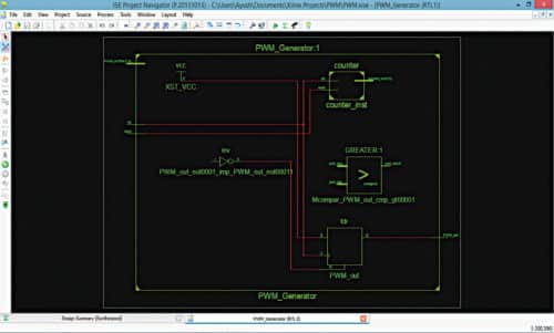
Block diagram of the PWM generator is shown in Fig. 1. Working principle of the generator is simple. It uses one counter and one comparator. The microcontroller unit provides 8-bit input into PWM module. Counter used in the PWM module is 8-bit. It increments its value on the positive edge of the clock (positive edge triggered). Comparator used in the PWM generator is also 8-bit.
Input given to PWM module is compared to the current value of the counter using the comparator. If current value of the counter is greater than the value given to the module as input, PWM output is pulled low. However, if current value of the counter is less than the value given as input to the module, output of PWM generator is pulled high.
Let us take a test case to understand the operation. Suppose, input to PWM module is 128 (10000000b). Counter is initialised using Reset button, so that output is 0(00000000b). During the first clock cycle, value of counter and input value to PWM module are compared.
The module finds that, value of counter is less than the value provided. This prompts the module to pull output of PWM generator high. This same paradigm keeps output of the generator pulled high until value of the counter reaches 128 (10000000)b.
In the next clock cycle, after the counter has reached 128, counter increments its value to 129(10000001)b. Comparator finds that, current counter value is greater than the value provided to PWM module, therefore output must be pulled low.
Changing input to PWM module will consequently change the threshold value, where transition from high to low state occurs. Thus, PWM can be achieved by varying the input provided to PWM module.
Verilog Code for PWM Generator
Verilog main code used (PWM_main.v) for PWM generation is given below.
module PWM_generator (PWM_ontime, PWM_out ,
clk , reset);
input clk, reset; // Port type declared
input [7:0] PWM_ontime; // 8-bit PWM input
output reg PWM_out; // 1 bit PWM output
wire [7:0] counter_out; // 8-bit counter
output
always @ (posedge clk)
begin
if (PWM_ontime > counter_out)
PWM_out <= 1;
else
PWM_out <= 0;
end
counter counter_inst(
.clk (clk),
.counter_out (counter_out),
.reset(reset)
);
endmodule
module counter(counter_out,clk,reset);
output [7:0] counter_out;
input clk, reset;
reg [7:0] counter_out;
always @(posedge clk)
if (reset)
counter_out <= 8’b0;
else
counter_out <= counter_out + 1;
endmodule
Software Simulation
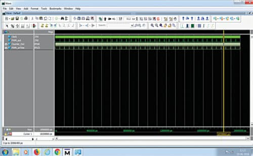
To check simulation output of the above code, use a simulation tool like ModelSim along with the test bench code (PWM_tb.v). Code simulation is done on Windows 7 using ModelSim v10.4a Student Version. Screenshot of the output is shown in Fig. 2.
Hardware Simulation
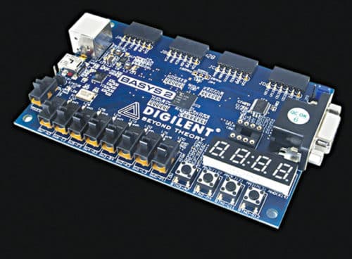
Module for PWM generator can be realised using Basys 2 development board (Fig. 3). The board is built around Xilinx Spartan-3E FPGA and Atmel AT90USB2 USB controller. It provides complete, ready-to-use hardware suitable for hosting circuits, ranging from basic logic devices to complex controllers.
This board is used, along with the following two software programs, to allow for effortless programming and debugging of the FPGA board:
1. Xilinx ISE Webpack 14.7
2. Digilent Adept v2.0 or higher
Digilent Adept v2.0 program allows USB programming through the computer USB port. The program, when run, automatically detects the development board connected to the system, and allows you to program ROM memory in the FPGA board to permanently store the code, or to temporarily program the FPGA with the code.
When programmed temporarily, FPGA runs the code as long as it is supplied with power. Once power disconnected, FPGA reverts back to being a blank IC, waiting to be programmed again.
Adept software requires a bitmap file with .bit extension. This is usually created using synthesiser software like ISE from Xilinx or Synplify from Synopsys for logical synthesis. This is where Xilinx ISE webpack is used, is a free software that can be used by anyone. Include the Verilog file into a new project along with a user constraints file (.ucf extension).
A user constraints file (PWM_ucf.ucf) binds the signals of the module to specific pins on the FPGA. The user constraints file for realising the same is as given below.
NET “PWM_out” LOC = “B2”;
NET “clk” LOC = “B8”;
NET “reset” LOC = “G12”;
NET “PWM_ontime<0>” LOC = “P11”;
NET “PWM_ontime<1>” LOC = “L3”;
NET “PWM_ontime<2>” LOC = “K3”;
NET “PWM_ontime<3>” LOC = “B4”;
NET “PWM_ontime<4>” LOC = “G3”;
NET “PWM_ontime<5>” LOC = “F3”;
NET “PWM_ontime<6>” LOC = “E2”;
NET “PWM_ontime<7>” LOC = “N3”;
After including the necessary files onto the project, select the option to generate a programming file, which creates .bit file that we require.
Launch Adept program and burn .bit file onto the FPGA for verification first and then onto the ROM so that FPGA works as a PWM module whenever powered on.
To test the circuit for functional verification, program 8-bit input of PWM generator as eight switches (SW0 through SW7) present on FPGA board. The board provides a 50MHz default clock attached to the FPGA through pin B8 (available at jumper header JP4). Output is taken from first pin B2 of first expansion header JA.
To verify output, connect an oscilloscope to the output of PWM generator at pin B2. The On pulse width will change in accordance to 8-bit binary sequence produced by toggling switch positions on the FPGA board. A reset button (G12) is provided on the board to restart the counter, if needed.
This PWM has a maximum operating frequency of 232.504MHz, which allows the most dynamic and fast operation applications to be accommodated. Total power dissipated by the design at an operation frequency of 50MHz is 38mW.
Static power dissipation for 34mW (power required to drive the development board) and the power consumed by the oscillator to produce the clock is 1mW. Average power consumed by PWM output is 3mW, which indicates that the design is also power efficient.
Download source code
Ayush Mallik is an electronics hobbyist and a circuit designer.

Sir, Thank you for the informative article. How can I modify the code for generating Sinusoidal pulse width modulation?