


Audio amplifiers are essential components in various electronic devices, ranging from smartphones and gaming consoles to gadgets and audio systems. They play a crucial role in converting low-power audio signals into audible sounds through speakers.
While commercial audio amplifiers can be expensive, today we’ll explore a cost-effective solution for designing a stereo audio amplifier circuit under 50 rupees using the PAM8403 chip.
This project offers features such as volume control, mute option, and stereo input/output capability.

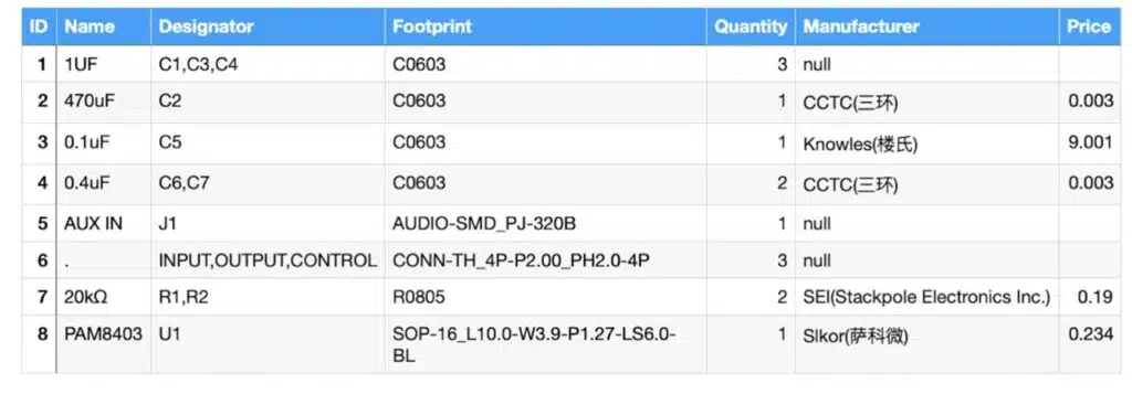
Bill of Materials
IC Configuration
According to the PAM8403 IC datasheet, the IC comes in a SOT-16 package with 16 pin. The IC can work with 5V input.
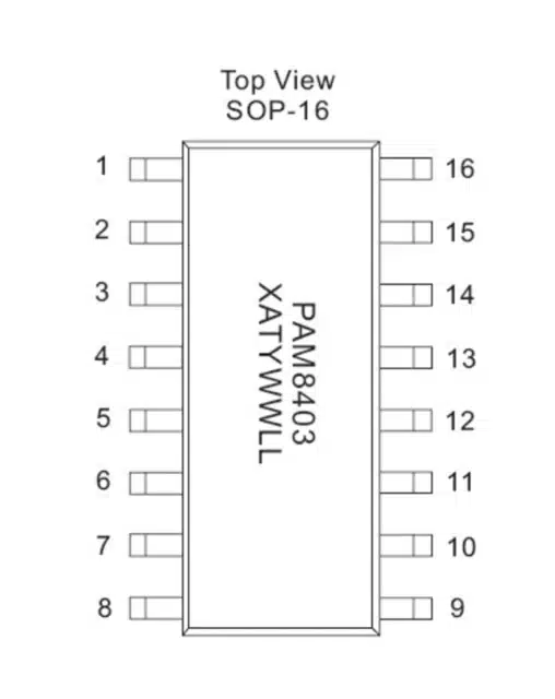
PAM8403 Pin Configuration:
- L-OUT (Pin 1): Left Channel Output – Connects to the positive terminal of the left speaker.
- L-GND (Pin 2): Left Channel Ground – Connects to the ground terminal of the left speaker.
- SD (Pin 3): Shutdown Pin – Connect to ground to enable the IC and disconnect to shut down the IC (optional).
- VDD (Pin 4): Power Supply (5V) – Connect to the positive terminal of the power supply.
- AGND (Pin 5): Analog Ground – Connect to the ground.
- RGND (Pin 6): Right Channel Ground – Connects to the ground terminal of the right speaker.
- R-OUT (Pin 7): Right Channel Output – Connects to the positive terminal of the right speaker.
- FLT (Pin 8): Filter Pin – Connect to ground for the default filter; floating or connected to VDD for a higher filter cutoff frequency.
- INL- (Pin 9): Negative Input for Left Channel.
- INL+ (Pin 10): Positive Input for Left Channel.
- INR+ (Pin 11): Positive Input for Right Channel.
- INR- (Pin 12): Negative Input for Right Channel.
- L- (Pin 13): Connect to the low terminal of the volume control potentiometer for the left channel.
- L+ (Pin 14): Connect to the high terminal of the volume control potentiometer for the left channel.
- R+ (Pin 15): Connect to the high terminal of the volume control potentiometer for the right channel.
- R- (Pin 16): Connect to the low terminal of the volume control potentiometer for the right channel.
As per datasheet, the IC need few decoupling capacitor and bypass capacitor with the IC. Here are the discrete components we need to add in the circuit.

1. Power Supply Decoupling:
- Use two capacitors of different types to target different types of noise.
- For higher frequency transients, spikes, or digital hash, employ a low ESR ceramic capacitor (typically 1.0μF) close to the VDD terminal.
- For filtering lower frequency noise signals, use a larger capacitor (20μF or greater) near the audio power amplifier.
2. Input Capacitor (CI):
- The input capacitor (CI) and input resistance (RI) form a high-pass filter.
- The corner frequency is determined by the equation:
- Consider the trade-off between cost, size, and low-frequency response when selecting the input capacitor size.
3. Analog Reference Bypass Capacitor (CBYP):
- CBYP is critical for startup and noise reduction.
- During start-up or recovery from shutdown, CBYP determines the rate at which the amplifier starts up.
- It reduces noise caused by power supply coupling into the output drive signal.
- Recommended values for CBYP are 0.47μF to 1.0μF for optimal THD and noise performance.
4. Under Voltage Lock-Out (UVLO):
- The PAM8403 has circuitry for detecting low supply voltage (2.0V or below).
- When the supply voltage is low, the outputs are disabled, and normal function resumes when VDD ≥ 2.2V.
5. Short Circuit Protection:
- The PAM8403 has short circuit protection to prevent damage during output-to-output or output-to-GND shorts.
- Outputs are immediately disabled upon short circuit detection.
- The device activates again if the short is removed.
6. Over Temperature Protection:
- Thermal protection prevents damage when the internal die temperature exceeds +140°C.
- There is a 15-degree tolerance on the trip point.
- The thermal fault is cleared once the die temperature is reduced by 30°C.
- This large hysteresis prevents motor boating sound, and normal operation resumes without external intervention.
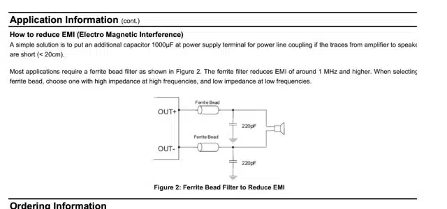
In addition, if you face any EMI interference, you can add the ferite with capacitor to reduce the noise and distortion in output sound but this is optional. Here is the detail from the datasheet of IC.
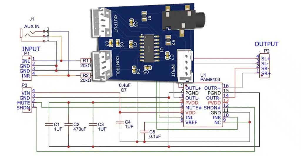
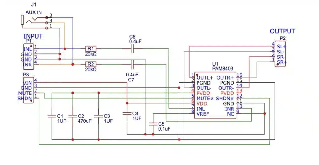
Stereo Audio Amplifier Circuit
So by combining the discrete components to stated pins we can add few connector and a TTRRS connector with IC to make a amplifier module. Here is the complete circuit diagram.
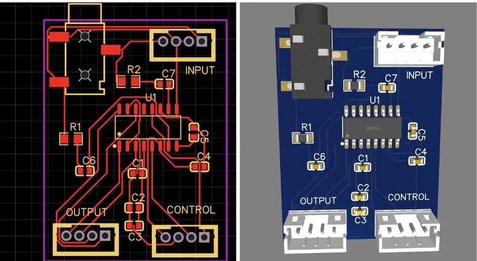
Designing the PCB
Next, we will proceed to design the PCB and connect the tracks. In this process, we will utilize a single top layer for both track layout and component placement.
Stereo Audio Amplifier Testing
Connect the device with 5V, then Connect the input sound signal wire to the input and then connect the speakers to the output and you get the amplified audio as output.
Other Stereo Amplifier Projects
- Hi-Fi Stereo Audio Power Amplifier
- 5W Stereo Amplifier
- Simple Audio Amplifier With Dual Power Source
You can download the reference Gerber file below.