


While very-large-scale integration (VLSI) and complementary metal oxide semiconductor (CMOS) technologies have had an exponential growth, energy-storage technologies have grown slowly, requiring improvement in electronic circuit designs. Today, such ICs are embedded in all kinds of electronic devices. These devices work on direct current (DC), which is often derived from alternating current (AC) mains supply. The conversion process using an AC adaptor, or a battery itself, consumes significant amount of power.
High power consumption areas
Power consumption is often directly related to performance. Higher the power available for consumption, the better can be the performance of the device. Hrishikesh Kamat, chief executive officer, Shalaka Technologies, says, “Optimising speeds and performance is a challenge.” A wearable device performing powerful functions, for example, would result in high power consumption. Lowering power consumption would limit its functions.
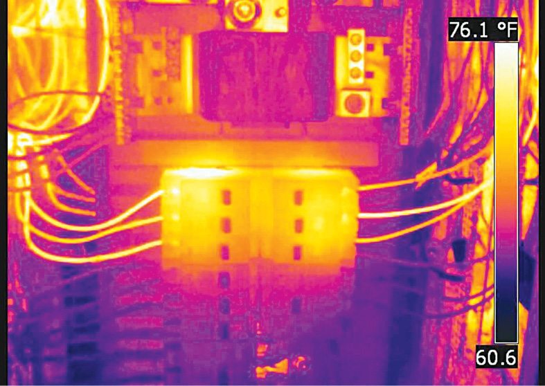
Losses through heat are a significant part of power consumption. “For smaller devices, heat losses are negligible or sometimes almost non-existent,” says T. Anand, managing director, Knewron Technologies. This becomes a problem in bigger devices where lot of power is lost through heat, requiring heat-sinks. Although higher speeds also cause higher power consumption, it is better to work faster in a short span of time. The device can go to sleep mode, whenever feasible, to reduce power consumption.

A step in this regard has been the introduction of low-power microcontroller modules. “Cortex M4 architecture based controllers are coming with deep sleep and hibernation,” says Kamat. “You can increase power consumption temporarily with an interrupt, and the system goes back to using lesser power.”
CMOS circuits for low power
With increase in integration, size and complexity of chips, thermal management is adding significant cost to the electronic products. Dynamic power dissipation in ICs does not increase much beyond 65nm, while static or leakage power also more or less remains the same. Localised dynamic power consumption can be reduced by providing different frequency clocks to different blocks of an IC.
Threshold voltages in CMOS cells also govern IC’s characteristics. Sub-threshold current in a CMOS IC reduces when threshold voltage is increased. Cells with a higher voltage can help in the reduction of sub-threshold current. Combining low- and high-voltage cells to reduce leakage current, while maintaining the desired frequency of operation, is a typical design trend.
High-voltage cells are used as ‘sleep’ transistors, which gate the supply to further low-voltage based designs when the block is in standby mode. Sleep transistors are turned on, resulting in low-voltage blocks downstream, during active mode.
Design trends, with a catch. By varying bias voltage using a control circuit, voltage can be dynamically changed as per the required application. It requires much complex MOS fabrication in twin-well or triple-well fabrication techniques, more commonly known as variable threshold CMOS (VTCMOS).
Lowering voltage, however, compromises with the reliability of the chip, causing voltage swings. These voltage swings can arise due to various process or environmental variations.
Dynamic voltage can also be reduced for supply voltage, which again has its downside. Reduction in supply voltage increases the delay of the cell as well. A balance has to be maintained between supply voltage and device performance.
Static voltage scaling presents a few constraints while operating electronics. It does not allow changes in the supply blocks once designed, hence, is not adaptive.
Adiabatic circuits are interesting in this regard. Here, energy spent to flip a bit can be reduced to very small values by externally controlling the length and shape of signal transitions.
An IC to reduce power consumption by 90 per cent. An adiabatic logic circuit can use AC voltage as its power source without converting it to DC voltage. Yasuhiro Takahashi, department of electrical electronic and computer engineering, Gifu University, Japan, has built a prototype that could be installed in healthcare products. The 155µm×172µm chip operates on AC.
The need arose from central processing units (CPUs) operating at high frequency levels of 500MHz, thereby rendering the circuits not advantageous for computing purposes. Interestingly, such a circuit could be used in healthcare devices or wristwatches that did not process at high speed. However, there are other methods for regular applications.
Low-power design techniques
Transistors are usually arranged in a plane structure, but applying a spatial structure and the adiabatic logic circuit could reduce power loss and thus power consumption. “Powering down various modes, not adding unnecessary parts and others must be taken care of while designing the circuit,” explains Anand. He adds, “Besides the hardware design and supporting components, overall functioning and the firmware code also contribute to power saving of the device.”
Either through architecture design that uses low-power techniques, or by adopting a process that can reduce consumption, designers always look for ways to reduce power consumption. Kamat explains, wireless systems consume a lot of power in transmission. He says, “The rate of transfer of information can be controlled and helps in minimising power consumption. Sampling rate of power consumption is reduced to increase power capacity.” Some of the solutions come at an expense in performance, reliability or chip area.
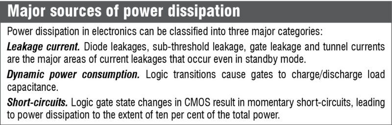
Making compromises in system design. Changing system architecture has been the most common technique for reducing power consumption. Clock gating is a very popular dynamic power-reduction technique. Power consumed during device logic switching and charging load capacitance are the major areas of concern.
Latch based clock gating is an interesting technique that saves designs from hazards that can lead to additional power consumption. The clock can be turned off when not needed. Modern EDA tools identify the circuits where clock gating can be inserted.
Traditional methods control the selection on a multiplexer. Latch based clock gating adds a level-sensitive latch to circuit design. It enables signal from the active edge of the clock until the inactive edge of the clock. Interestingly, clock gating does not require modifications to the RTL description.
Selection of components. “Selection of components for low-power devices involves two critical parameters,” explains Anand. Low quiescent current as well as lower operating power need to be calculated, and the component’s power should be controllable.
“Controlling the component allows turning off the device, put it into lower-power mode or disable it using external control.”
Multiple voltages. Another trick to save power is to operate different areas of the circuit at different voltages. In any circuit, there are specific areas that operate at high voltages, whereas other parts can work well at lower voltages for major power savings. This also reduces leakage power.
Power gating is a technique implemented in devices with sleep mode. In certain instances, only part of the device is required to function. It makes sense to switch off non-functional blocks to save power. Leakage power and dynamic consumption can be reduced in such power-gated blocks. However, power coming from power-reduced blocks should not affect the functioning blocks. Hence, the design has to incorporate isolation blocks, so that functionality corruption does not occur.
The demand
Mobile device consumers require longer talk and standby times with extended battery life at lower cost. Demand for smaller and sleeker devices has been resulting in higher levels of silicon integration in advanced processes. However, higher leakage current in advanced processes requires a reduction to reduce power consumption. Losses through heat are also being managed with some ingenious solutions. “Energy dissipation in the form of heat can also be used to generate power,” says Kamat.
Saurabh Durgapal is working as technology journalist at EFY

I am looking for a DIY or assembled kit form APFC for 1.5KW Single Phase and 4KW Three Phase domestic power supply. There are some published in EFY, but they are not available in kit form. Also these circuits never recommend any practically available capacitors to be used in them.